
Version 2.3, April 8, 2003
Proprietary to OmniVision Technologies
1
Advanced Information
Preliminary Datasheet
OV8610 Color CMOS SVGA (800 x 600) C
AMERA
C
HIPTM
O
mni
TM
ision
General Description
The OV8610 CMOS image sensor is a single-chip
video/imaging camera device designed to provide a high
level of functionality in a single, small-footprint package.
The device incorporates an 800 x 600 image array
capable of operating at up to 15 frames per second (fps)
in full resolution. Proprietary sensor technology utilizes
advanced algorithms to cancel Fixed Pattern Noise
(FPN), eliminate smearing, and drastically reduce
blooming. All required camera functions including
exposure control, gamma, gain, white balance, color
matrix, color saturation, hue control, windowing, and
more, are programmable through the serial SCCB
interface. The device can be programmed to provide
image output in different 8-bit or 16-bit digital formats.
Features
�
480,000 pixels, 1/3" lens, SVGA/QSVGA format
�
Data output formats include:
�
ITU-601
�
ITU-656
�
Choice of progressive scan/interlaced read
�
Wide dynamic range, anti-blooming, zero smearing
�
Electronic exposure/gain/white balance control
�
Image quality controls - brightness, contrast, gamma,
saturation, sharpness, windowing, hue, etc.
�
Internal and external synchronization
�
Line exposure option
�
3.3-Volt operation, low power dissipation
�
< 30 mA active power at 30 fps with 10 mA load
�
< 10 �A in power-down mode
�
Built in Gamma correction (0.45/1.00)
�
SCCB programmable:
�
Color saturation, brightness, hue, white balance,
exposure time, gain, etc.
Ordering Information
Product
Package
OV8610 (Color, SVGA, QSVGA,
QQSVGA)
CLCC-48
Applications
�
Cellular phones
�
Digital still cameras
�
PC Multimedia
�
PDAs
�
Machine vision
Key Specifications
Figure 1 OV8610 Pin Diagram
Array Size
SVGA 800 x 600
QSVGA 400 x 300
Power Supply 3.0 - 3.6 VDC
Power
Requirements
Active < 30 mA (with 10 mA load)
Standby < 10 �A
Electronics Exposure Up to 648:1 (for selected fps)
Output Format 10-bit digital raw RGB data
Lens Size 1/3"
Max. Image
Transfer Rate
SVGA 15 fps
QSVGA 30 fps
Min. Illumination (3000K) < 3 lux @ f1.2
S/N Ratio > 48 dB (AGC off,Gamma=1)
Dynamic Range > 72 dB
Scan Mode Progressive or Interlaced
Gamma Correction On/Off 0.45/1.0
Pixel Size 6.2 �m x 6.2 �m
Dark Current < 0.2 nA/cm
2
Fixed Pattern Noise < 0.03% of V
PEAK-TO-PEAK
Image Area 4.96 mm x 3.72 mm
Package Dimensions .560 in. x .560 in.
36
Y5/
SHARP
37
Y4
38
Y3/RGB
39
Y2/G2X
40
Y1/PROG
41
Y0/CBAR
42
CHSYNC/
BW
31
DOGND
32
DOVDD
33
PCLK/
PWDB
34
Y7
35
Y6
13 VTO
12 SCCBB
11 VcCHG
10 HVDD
9
PWDN
8
AVDD
7
AGND
18 HREF/
VFLIP
17 FODD/
SRAM
16
VSYNC/
CSYS
15 ADGND
14 ADVDD
48
SG
N
D
1
SV
D
D
2
R
E
SE
T
3
AG
C
E
N
4
FR
E
X
5
VR
EQ
6
AS
UB
43
DE
G
N
D
44
DE
V
D
D
45
SI
O
_
1
46
SI
O
_
0
47
RS
V
D
OV8610
25
UV
1
/
CC
6
5
6
24
UV
2
/
Q
S
VG
A
23
UV
3
/
EC
L
K
0
22
UV
4
/
SL
A
E
N
21
UV
5
/
M
I
R
20
UV
6
/
TV
E
N
19
UV
7
/
B8
30
DG
N
D
29
DV
DD
28
XC
L
K
2
27
XC
L
K
1
26
UV
0
/
GA
M
M
A
2
Proprietary to OmniVision Technologies
Version 2.3, April 8, 2003
OV8610
Color CMOS SVGA (800 x 600) C
AMERA
C
HIP
TM
O
mni
ision
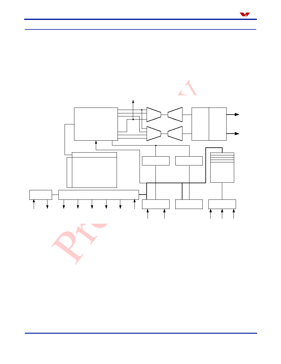
Functional Description
Figure 2
shows the functional block diagram of the OV8610 image sensor. The OV8610 includes:
�
Image Sensor Array
(824 x 615 resolution)
�
Analog Signal Processor
�
Dual 10-Bit Analog-to-Digital Converters
�
Digital Data Formatter
�
Video Port
�
SCCB Interface
Figure 2 Functional Block Diagram
Image Array
(824 x 615)
B
R
VTO
G
MUX
A/D
A/D
Digital
Data
Formatter
Video
Port
Y[7:0]
Cr
Y
Cb
MUX
Analog Signal
Processor
Exposure/Gain
Detect
White Balance
Detect
Exposure/Gain
Control
White Balance
Control
SCCB
Interface
Column Sense Amp
Ro
w
S
e
l
e
c
t
Video Timing Generator
XCLK2
XCLK1
Clock
SCCBB
SIO_0
SIO_1
Control
Registers
.
.
.
.
UV[7:0]
HREF/
VSFRAM
PCLK/
PWDB
VSYNC
FODD CHSYNC
MIR
AGCEN
PROG
Image Sensor Array
The OV8610 sensor is a 1/3" CMOS imaging device. The
sensor contains a total of 506,760 pixels (824 x 615). Its
design is based on a field integration readout system with
line-by-line transfer and an electronic rolling shutter with a
synchronous pixel readout scheme. The color filter of the
sensor consists of primary red, green, and blue filters
arranged in the line-alternating Bayer pattern,
RGRG/GBGB.
Analog Signal Processor
The image is captured by the 824 x 615 pixel image array
and routed to the analog processing section where the
majority of signal processing occurs. This block contains
the circuitry that performs color separation, color
correction, automatic gain control (AGC), gamma
correction, color balance, black level calibration, aperture
correction, controls for picture luminance and
chrominance, and hue control for color. The analog video
signals are based on the following formula:
Y = 0.59G + 0.31R + 0.11B
U = R - Y
V = B - Y
where R, G, B are the equivalent color components in
each pixel.
YCbCr format is also supported, based on the following:
Y = 0.59G + 0.31R + 0.11B
Cr = 0.713 (R - Y)
Cb = 0.564 (B - Y)

Functional Description
Version 2.3, April 8, 2003
Proprietary to OmniVision Technologies
3
O
mni
ision
Dual 10-Bit Analog-to-Digital Converters
The YCbCr or RGB data signal from the analog
processing section is fed to two on-chip 10-bit
analog-to-digital (A/D) converters: one for the Y/G
channel and one shared by the CbCr/BR channels.
The on-chip 10-bit A/D operates at up to 20 MHz, and is
fully synchronous to the pixel rate. Actual conversion rate
is related to the frame rate. A/D black-level calibration
circuitry ensures:
�
Black level of Y/RGB is normalized to a value of 16
�
Peak white level is limited to 240
�
CbCr black level is 128
�
CbCr Peak/bottom is 240/16
�
RGB raw data output range is 16/240
NOTE: Values 0 and 255 are reserved for sync flag
Digital Data Formatter
The converted data stream is further conditioned in the
digital formatter. The processed signal is delivered to the
digital video port through the video multiplexer which
routes the user-selected 8-, or 10-bit video data to the
correct output pins.
Image Processing
The algorithm used for the electronic exposure control is
based on the brightness of the full image. The exposure is
optimized for a "normal" scene that assumes the subject
is well lit relative to the background. In situations where
the image is not well lit, the automatic exposure control
(AEC) white/black ratio may be adjusted to suit the needs
of the application.
Additional on-chip functions include:
�
AGC that provides a gain boost of up to 24 dB
�
White balance control that enables setting of proper
color temperature and can be programmed for
automatic or manual operation.
�
Separate saturation, brightness, hue, and sharpness
adjustments allow for further fine-tuning of the picture
quality and characteristics.
The OV8610 image sensor also provides control over the
White Balance ratio for increasing/decreasing the image
field Red/Blue component ratio. The sensor provides a
default setting that may be sufficient for many
applications.
Windowing
The windowing feature of the OV8610 image sensor
allows user-definable window sizing as required by the
application (see
Figure 3
). Window size setting (in pixels)
ranges from 2 x 2 to 800 x 600, and can be positioned
anywhere inside the 824 x 615 boundary. Note that
modifying window size and/or position does not change
frame or data rate. The OV8610 image sensor alters the
assertion of the HREF signal to be consistent with the
programmed horizontal and vertical region. The default
output window is 800 x 600.
Figure 3 Windowing
Zoom Video (ZV)
The OV8610 image sensor includes a Zoom Video (ZV)
function that supports standard ZV port interface timing.
Signals available include VSYNC, CHSYNC, PCLK and
16-bit data bus: Y[7:0] and UV[7:0]. The rising edge of
PCLK clocks data into the ZV port (see
Figure 6
).
QSVGA-Skip
A QSVGA mode is available for applications where higher
resolution image capture is not required. Only half of the
pixel rate is required when programmed in same frame
rate with sub-sampling method. If retaining the same pixel
rate with the skip method, the maximum frame rate is 120.
Default resolution is 400 x 300 pixels and can be
programmed for other resolutions. Refer to
Table 6
and
Table 7
for further information.
Column
End
Sensor Array
Boundary
HREF
HR
E
F
Column
Display
Window
Column
Start
Row Start
Row End
R
o
w

4
Proprietary to OmniVision Technologies
Version 2.3, April 8, 2003
OV8610
Color CMOS SVGA (800 x 600) C
AMERA
C
HIP
TM
O
mni
ision
QQSVGA-Skip
A QQSVGA mode is available for further resolution
decrease. Two methods are used to get this mode,
sub-sampling and skip. Sub-sampling can get better
quality than skip but skip can attain a higher frame rate.
The maximum frame rate is 240 for QQSVGA and the
default resolution is 200 x 150.
Video Port
The video output port of the OV8610 image sensor
provides a number of output format/standard options to
suit many different application requirements.
Table 1
indicates the output formats available. These formats are
user-programmable through the SCCB interface.
YUV Output
The OV8610 supports ITU-656 and ITU-601 output
formats, providing VSYNC, HREF, and PCLK as standard
output video timing signals.
ITU-601/ITU-656
The OV8610 image sensor supports both ITU-601 and
ITU-656 output formats in the following configurations
(see
Table 3
and
Figure 4
for further details):
16-bit, 4:2:2 Format
This mode complies with the 60/50 Hz ITU-601 timing
standard (see
Table 3
).
8-bit data mode
In this mode, video information is output in Cb Y Cr Y
order using the Y port only and running at twice the pixel
rate during which the UV port is inactive (see
Table 2
).
The OV8610 image sensor provides VSYNC, HREF,
PCLK, FODD, and CHSYNC as standard video timing
signals.
In ITU-656 modes, the OV8610 image sensor asserts
Start of Active Video (SAV) and End of Active Video (EAV)
to indicate the beginning and ending of the HREF window.
As a result, SAV and EAV change with the active pixel
window.
The OV8610 image sensor offers flexibility in YUV output
format. The device may be programmed to standard YUV
4:2:2. The device may also be configured to "swap" the
UV sequence. When swapped, the UV channel output
sequence in the 16-bit configuration becomes:
V U V U���
The 8-bit configuration becomes:
V Y U Y���.
The third format available in the 8-bit configuration is the
Y/UV sequence swap:
Y U Y V���.
RGB Raw Data Output
The OV8610 image sensor can also be programmed to
provide 8-bit RGB raw data output. The output sequence
is matched to the OV8610 color filter pattern.
The video output appears in Y channel only and the UV
channel is disabled in 8-bit RGB raw data. The output
sequence is B G R G.

Functional Description
Version 2.3, April 8, 2003
Proprietary to OmniVision Technologies
5
O
mni
ision
Table 1
Digital Output Formats
Resolution
Pixel Clock
800 x 600
400 x 300
200 x 150
YUV
16-bit
Y
a
a.
"Y" indicates mode/combination is supported by the OV8610
Y
Y
8-bit
Y
Y
Y
ITU-656
Y
Y
Y
RGB
16-bit
Y
Y
Y
8-bit
Y
Y
Y
ITU-656
b
b.
Output is 8-bit in RGB ITU-656 format. SAV and EAV are inserted at the beginning and ending of HREF, which synchronizes the ac-
quisition of VSYNC and HSYNC. 8-bit data bus configuration (without VSYNC and CHSYNC) can provide timing and data in this format.
Y
Y
Y
Y/UV Swap
c
c.
Y/UV swap is valid in 8-bit format only. Y channel output sequence is Y U Y V.
16-bit
8-bit
Y
Y
Y
U/V Swap
YUV
d
d.
U/V swap means UV channel output sequence swaps in YUV format (i.e., V U V U ... for 16-bit and V Y U Y ... for 8-bit).
Y
Y
Y
RGB
e
e.
U/V swap means neighbor row B R output sequence swaps in RGB format. Refer to
RGB Raw Data Output
for further details.
Y
Y
Y
YG
16-bit
Y
Y
Y
8-bit
Single-Line RGB Raw Data
16-bit
8-bit
Y
Y
Y
MSB/LSB Swap
Y
Y
Y
Table 2
4:2:2 8-bit Format
Data Bus
Pixel Byte Sequence
Y7
U7
Y7
V7
Y7
U7
Y7
V7
Y7
Y6
U6
Y6
V6
Y6
U6
Y6
V6
Y6
Y5
U5
Y5
V5
Y5
U5
Y5
V5
Y5
Y4
U4
Y4
V4
Y4
U4
Y4
V4
Y4
Y3
U3
Y3
V3
Y3
U3
Y3
V3
Y3
Y2
U2
Y2
V2
Y2
U2
Y2
V2
Y2
Y1
U1
Y1
V1
Y1
U1
Y1
V1
Y1
Y0
U0
Y0
V0
Y0
U0
Y0
V0
Y0
Y Frame
0
1
2
3
UV Frame
0 1
2 3