 | –≠–ª–µ–∫—Ç—Ä–æ–Ω–Ω—ã–π –∫–æ–º–ø–æ–Ω–µ–Ω—Ç: C2306 | –°–∫–∞—á–∞—Ç—å:  PDF PDF  ZIP ZIP |
C2306
..
DATA
SHEET
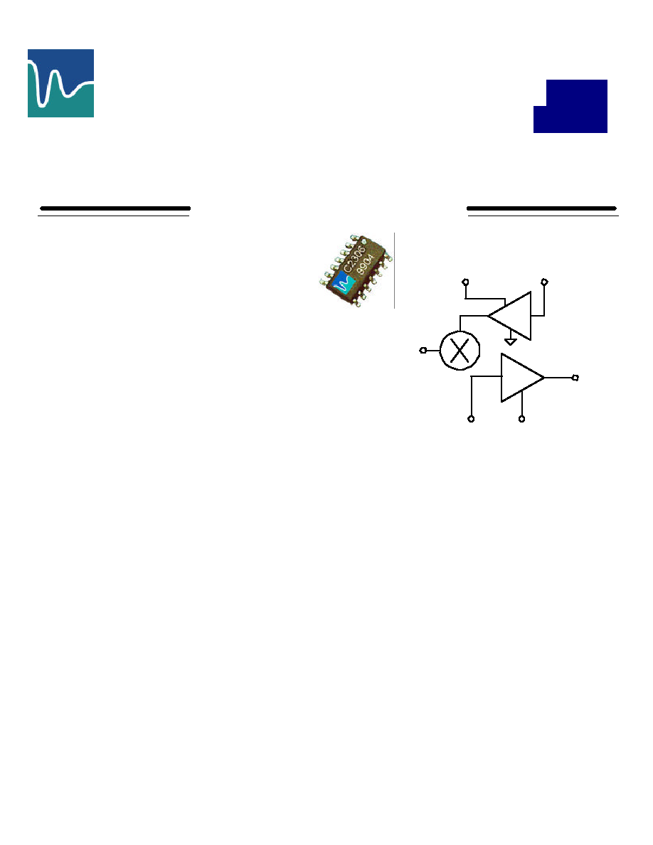
MMDS / ISM / S-Band Mixer
1800 to 4800 MHz Operation
Features
∑
10 dB Gain
∑
10 to 900 MHz Integrated IF Amplifier
∑
Single 5V Supply
∑
26 dBm Output IP3
∑
Separate MIXER/LO AMP and IF AMP cells.
∑
75 ohm IF output impedance
Applications
∑
2.4 GHz ISM Band Applications
∑
Wireless Local Loop Systems
∑
MMDS Downconverters
∑
Wireless LANS and WANS
∑
MMDS Upconverters
∑
Wireless Internet Systems
∑
Bluetooth Applications
∑
Wireless T1 Data Link Equipment
Description
The C2306 is a flexible, high intercept, frequency conversion GaAs MMIC packaged in a 14 pin SOIC
package. The MMIC is usable as an upconverter or downconverter mixer. Each subcircuit is brought out on
separate pins to allow for custom filtering on the IF/RF mixer interstage or custom matching for specific bands.
Broadband parallel feedback networks are used on the gain and LO driver stages and the mixer is a singly
balanced two diode mixer. The FET source of the IF amplifier stage (IF BIAS) is accessible for AC bypassing
which allows for current reduction with self bias circuitry. The gain and DC current is broken up as follows:
LO AMP gain = 11dB; current = 27 mA, IF AMP gain = 17dB, current = 60mA, Mixer conversion loss = -
6dB. Simple external matching circuits can be implemented for all ports to achieve VSWR's < 2:1 over
moderate bandwidths of less than 400MHz.
Pacific Wireless
2844 Mar Vista Dr. Suite 101
Aptos, CA 95003
TEL (831) 684-2474
FAX (831) 684-2494
www.pacwireless.com
LO IN
IF OUT
VDD
IF/RF
IF IN
IF BIAS
C2306
Specifications Subject to Change Without Notice C2306Spec Rev
5 12/30/9 9
Page 2
Electrical Characteristics
Typical Specifications for V
DD
=5.0V T
A
=+25
o
C
Minimum and Maximum specifications are guaranteed over RF range 2.50GHz ≠ 2.68GHz
Tested in 50
input / 75
output system, LO=2.278GHz at 5dBm, using matching circuit shown on page 2.
Parameter
Symbol
Conditions
Min
Typ
Max
Units
Conversion Gain
G
LO=5dBm
9
10
11
dB
Single Sideband Noise Figure
NF
LO=2.278GHz
12
dB
Output IP3
IP3
LO=5dBm
26
dBm
IF Output Return Loss
S
22
75
output ref.
-11
dB
LO Input Return Loss
S
11
50
input ref.
-2
dBm
Output Power at 1dB Comp.
P
1dB
LO=5dBm
17
dBm
Operating Drain Current
I
DD
85
mA
LO IN to IF OUT Isolation
ISO
l-i
LO=5dBm
-40
dB
Load VSWR for Input/Output
Stability
1
VSWR
With network on page 2
10:1
Thermal Resistance
JC
Junction to GND lead
75
∞
C/W
1
As a separate circuit the IF AMP is conditionally stable for VSWR < 5:1 over 1.5-3.6GHz
Absolute Maximum Ratings
Characteristic
Symbol
Value
Units
Drain Voltage
V
DD1,2
+7
V
Bias Current
I
DS
160
mA
RF Input Power
P
IN
+18
dBm
Power Dissipation
P
DISS
.6
W
Load VSWR
VSWR
10:1
Operating Temperature
T
OP
-40 to +85
∞
C
Junction Temperature
T
J
150
∞
C
Storage Temperature Range
T
STG
-65 to +150
∞
C
Caution: Operating beyond specified rating for any of these parameters may cause permanent damage to the device.
Application Information
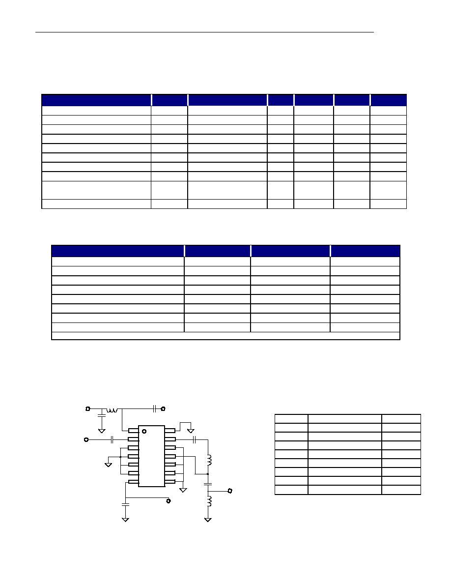
Matching/Diplexing Circuit for 2.5 to 2.68 GHz Operation
PM2117
C2306
1
2
3
4
5
6
7
8
9
10
11
12
13
14
VDD
+5V
LO IN
IF OUT
C1
C3
C4
C5
L2
C2
VDD
+5V
RF IN
L1
L3
C7
Part
Value/Type
Size
C1
270pF NPO
0603
C2
200pF NPO
0603
C3
33pF NPO
0603
C4,C7
0.1uF X7R
0603
C5
1.8pF NPO
0603
L1
5 nH
0805
L2
560 nH
1008
L3
15 nH
0805
C2306
Specifications Subject to Change Without Notice C2306Spec Rev
5 12/30/9 9
Page 3
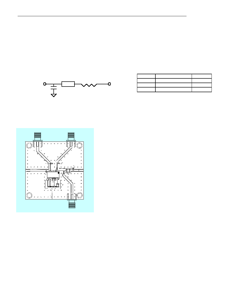
Recommended LO IN Port Matching
The LO IN port of the C2306 can be matched into 50 ohms with a lossy network. At 3dBm drive, the
unmatched port is at Z = 5 ≠15j ohms at 2.278 GHz. Also of note is that this impedance varies somewhat with
the LO drive level. Therefore a narrow band high Q network is not recommended due to inherent
manufacturing variation in LO drive available. The simple network below matches this port over an ~ 10%
bandwidth.
Test Board Layout
LO IN
Pin 2
C1
TRL 1
R1
LO Source
50 ohm
VDD
IF AMP
LO IN
RF IN
VDD
IF OUT
C230X
Material : GETEK
.028"
Biasing and Electrical Ground/
Thermal Considerations
Pins 3,4,5,10 and 12 should have ground vias straddling
both sides of the pin solder contact. This insures good
electrical and thermal grounding. If the IF AMP is run at
I
dss
(DC Grounded IF BIAS pin 14), this pin should be
grounded as described above. It is recommended that a
continuous ground plane be present under the package
to lower pin impedance and maintain similarity with the
matching environment used in the schematic in the
Application Information section. Bias for the IF amplifier
is supplied thru IF OUT pin 14. All ports are DC coupled
to the IC. Pins 2,6 and 13 should be kept at 0V DC to
maintain proper gate voltages. Pin 9 is internally biased
at 5V under normal operation and requires an external DC
block.
Part
Value/Type
Size
C1
1.8pF NPO
0603
R1
4.3
0603
TRL1
= 21
∞
, Z
0
=110
@2.5GHz
C2306
Specifications Subject to Change Without Notice C2306Spec Rev
5 12/30/9 9
Page 4
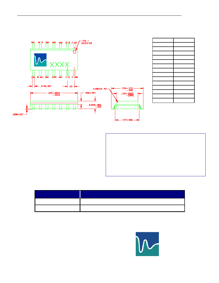
Package Specifications
Notes:
∑
Standard packaging is 14L SOIC tube. Tape and Reel
available upon request.
∑
All shipments F.O.B. Pacific Wireless Aptos, CA 95003
Part Numbers:
Part Number
Description
C2306
1800 to 4800 Mixer ≠ Tube
C2306TR
1800 to 4800 Mixer ≠ Tape and Reel
For further information contact:
C2306
Pacific Wireless
2844 Mar Vista Dr. Suite 101
Aptos, CA 95003
TEL (831) 684-2474
FAX (831) 684-2494
www.pacwireless.com
Pin Number
Function
1
IF OUT
2
LO IN
3
GND
4
GND
5
GND
6
GND
7
VDD
8
GND
9
GND
10
GND
11
IF/RF
12
GND
13
IF IN
14
IF BIAS
Advantages of GaAs MMIC
RF Integration ≠ Less Components/Board Space
Good Device Matching ≠ No Tweaks ≠ Less Tuning
Great power efficiency at low voltage
Better Linearity and Distortion Performance
Superb Radiation Immunity
No Latent or Cummulative ESD effects
No Infant Mortality; No "Walking Wounded"
No Burn-in Necessary