1
Transistor
2SC2671(F)
Silicon NPN epitaxial planer type
For UHF band low-noise amplification
s
Features
q
Low noise figure NF.
q
High gain.
q
High transition frequency f
T
.
s
Absolute Maximum Ratings
(Ta=25∞C)
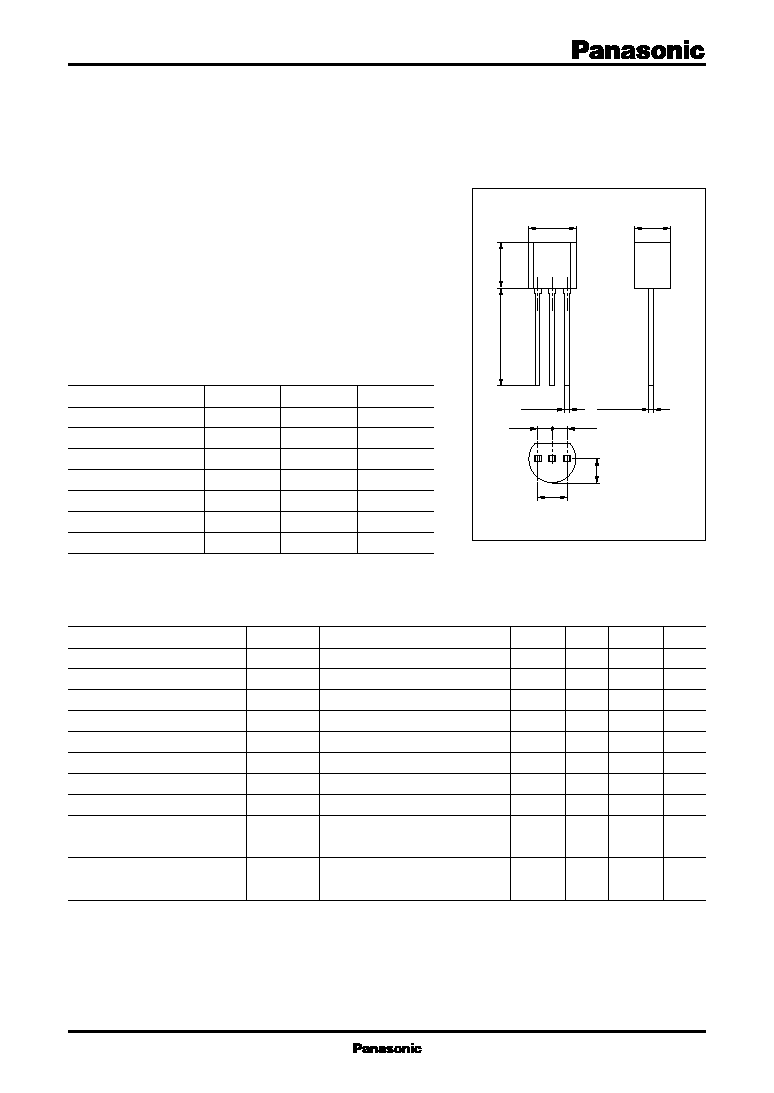
Unit: mm
Parameter
Collector to base voltage
Collector to emitter voltage
Emitter to base voltage
Collector current
Collector power dissipation
Junction temperature
Storage temperature
1:Base
2:Emitter
3:Collector
JEDEC:TO≠92
EIAJ:SC≠43A
5.0
±
0.2
4.0
±
0.2
5.1
±
0.2
13.5
±
0.5
0.45
+0.2
≠0.1
0.45
+0.2
≠0.1
1.27
1.27
2.3
±
0.2
2.54
±
0.15
2
1
3
Symbol
V
CBO
V
CER
*
V
EBO
I
C
P
C
T
j
T
stg
Ratings
15
14
2
80
600
150
≠55 ~ +150
Unit
V
V
V
mA
mW
∞C
∞C
s
Electrical Characteristics
(Ta=25∞C)
Parameter
Collector cutoff current
Emitter cutoff current
Forward current transfer ratio
Transition frequency
Collector output capacitance
Foward transfer gain
Maximum unilateral power gain
Noise figure
Second inter modulation distortion
Third inter modulation distortion
Symbol
I
CBO
I
EBO
h
FE
f
T
*
C
ob
*
| S
21e
|
2
GUM
*
NF
*
IM
2
*
IM
3
*
Conditions
V
CB
= 10V, I
E
= 0
V
EB
= 1V, I
C
= 0
V
CE
= 8V, I
C
= 40mA
V
CE
= 8V, I
C
= 40mA, f = 800MHz
V
CB
= 10V, I
E
= 0, f = 1MHz
V
CE
= 8V, I
C
= 40mA, f = 800MHz
V
CE
= 8V, I
C
= 40mA, f = 800MHz
V
CE
= 8V, I
C
= 40mA, f = 800MHz
V
CE
= 8V, I
C
= 40mA, f
1
= 200MHz
f
2
= 500MHz, V
O
= 100dB
µ
/75
V
CE
= 8V, I
C
= 40mA, f
1
= 600MHz
f
2
= 500MHz, V
O
= 100dB
µ
/75
min
50
3.5
9
10
50
75
typ
150
5.5
0.8
12
13
2.0
60
86
max
1
1
300
1.5
15
3.2
Unit
µ
A
µ
A
GHz
pF
dB
dB
dB
dB
dB
*
REB = 1k
*
LTPD = 10%
2
Transistor
2SC2671(F)
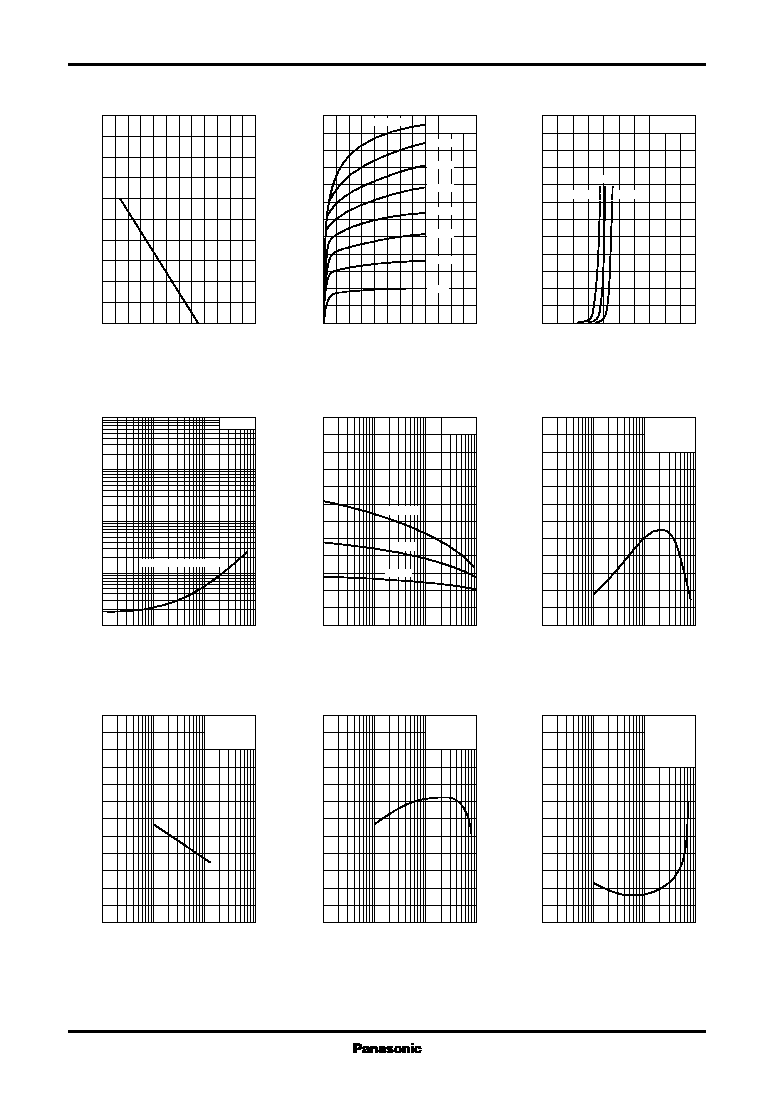
P
C
-- Ta
I
C
-- V
CE
I
C
-- V
BE
V
CE(sat)
-- I
C
h
FE
-- I
C
f
T
-- I
E
C
ob
-- V
CB
GUM -- I
C
NF -- I
C
0
240
200
160
40
120
80
0
1.0
0.8
0.6
0.4
0.2
Ambient temperature Ta (∞C)
Collector power dissipation P
C
(W
)
0
12
10
8
2
6
4
0
60
50
40
30
20
10
Ta=25∞C
350
µ
A
300
µ
A
250
µ
A
200
µ
A
150
µ
A
100
µ
A
50
µ
A
I
B
=400
µ
A
Collector to emitter voltage V
CE
(V)
Collector current I
C
(mA
)
0
2.0
1.6
0.4
1.2
0.8
0
120
100
80
60
40
20
V
CE
=8V
Ta=75∞C
≠25∞C
25∞C
Base to emitter voltage V
BE
(V)
Collector current I
C
(mA
)
0.1
1
10
100
0.3
3
30
0.01
0.03
0.1
0.3
1
3
10
30
100
I
C
/I
B
=10
Ta=75∞C, 25∞C, ≠25∞C
Collector current I
C
(mA)
Collector to emitter saturation voltage V
CE(sat)
(V
)
0.1
1
10
100
0.3
3
30
0
600
500
400
300
200
100
V
CE
=8V
Ta=75∞C
25∞C
≠25∞C
Collector current I
C
(mA)
Forward current transfer ratio h
FE
≠ 0.1
≠1
≠10
≠100
≠ 0.3
≠3
≠30
0
12
10
8
6
4
2
V
CB
=8V
f=800MHz
Ta=25∞C
Emitter current I
E
(mA)
Transition frequency f
T
(MHz
)
0.1
1
10
100
0.3
3
30
0
2.4
2.0
1.6
1.2
0.8
0.4
I
E
=0
f=1MHz
Ta=25∞C
Collector to base voltage V
CB
(V)
Collector output capacitance C
ob
(pF
)
0.1
1
10
100
0.3
3
30
0
24
20
16
12
8
4
V
CE
=8V
f=800MHz
Ta=25∞C
Collector current I
C
(mA)
Maximum unilateral power gain GUM
(dB
)
0.1
1
10
100
0.3
3
30
0
12
10
8
6
4
2
V
CE
=8V
(R
g
=50
)
f=800MHz
Ta=25∞C
Collector current I
C
(mA)
Noise figure NF
(dB
)