1
Transistor
2SC3354
Silicon NPN epitaxial planer type
For high-frequency amplification/oscillation/mixing
s
Features
q
Optimum for high-density mounting.
q
Allowing supply with the radial taping.
q
High transition frequency f
T
.
s
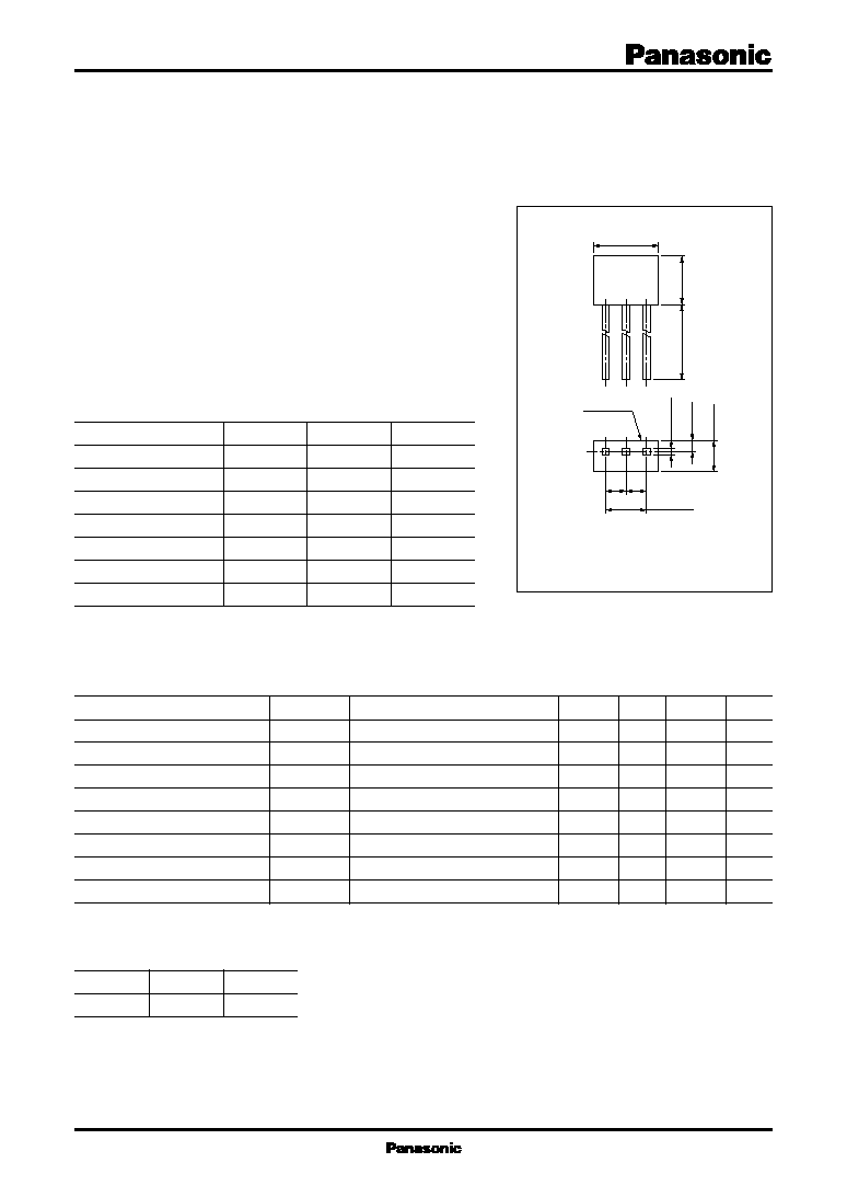
Absolute Maximum Ratings
(Ta=25∞C)
Unit: mm
Parameter
Collector to base voltage
Collector to emitter voltage
Emitter to base voltage
Collector current
Collector power dissipation
Junction temperature
Storage temperature
1:Emitter
2:Collector
EIAJ:SC≠72
3:Base
New S Type Package
4.0
±
0.2
marking
2.54
±
0.15
1.27
1.27
3.0
±
0.2
15.6
±
0.5
2.0
±
0.2
0.7
±
0.1
0.45
≠
0.1
1
2
3
+0.2
Symbol
V
CBO
V
CEO
V
EBO
I
C
P
C
T
j
T
stg
Ratings
30
20
3
50
300
150
≠55 ~ +150
Unit
V
V
V
mA
mW
∞C
∞C
s
Electrical Characteristics
(Ta=25∞C)
Parameter
Collector to base voltage
Emitter to base voltage
Forward current transfer ratio
Base to emitter voltage
Common base reverse transfer capacitance
Common emitter reverse transfer capacitance
Transition frequency
Power gain
Symbol
V
CBO
V
EBO
h
FE
V
BE
C
rb
C
re
f
T
*
PG
Conditions
I
C
= 100
µ
A, I
E
= 0
I
E
= 10
µ
A, I
C
= 0
V
CB
= 10V, I
E
= ≠2mA
V
CB
= 10V, I
E
= ≠2mA
V
CE
= 6V, I
C
= 0, f = 1MHz
V
CE
= 10V, I
C
= 1mA, f = 10.7MHz
V
CB
= 10V, I
E
= ≠15mA, f = 200MHz
V
CB
= 10V, I
E
= ≠1mA, f = 100MHz
min
30
3
25
600
typ
720
0.8
1
1200
17
max
250
1.5
1600
Unit
V
V
mV
pF
pF
MHz
dB
*
h
FE
Rank classification
Rank
T
S
f
T
(MHz)
600 ~ 1300
900 ~ 1600
2
Transistor
2SC3354
P
C
-- Ta
I
C
-- V
CE
I
C
-- V
BE
V
CE(sat)
-- I
C
h
FE
-- I
C
f
T
-- I
E
C
ob
-- V
CB
Z
rb
-- I
E
C
re
-- V
CE
0
160
40
120
80
140
20
100
60
0
500
400
300
200
100
Ambient temperature Ta (∞C)
Collector power dissipation P
C
(mW
)
0
12
10
8
2
6
4
0
60
50
40
30
20
10
Ta=25∞C
250
µ
A
200
µ
A
150
µ
A
100
µ
A
50
µ
A
I
B
=300
µ
A
Collector to emitter voltage V
CE
(V)
Collector current I
C
(mA
)
0
2.0
1.6
0.4
1.2
0.8
0
60
50
40
30
20
10
V
CE
=10V
Ta=75∞C
≠25∞C
25∞C
Base to emitter voltage V
BE
(V)
Collector current I
C
(mA
)
0.1
1
10
100
0.3
3
30
0.01
0.03
0.1
0.3
1
3
10
30
100
I
C
/I
B
=10
Ta=75∞C
25∞C
≠25∞C
Collector current I
C
(mA)
Collector to emitter saturation voltage V
CE(sat)
(V
)
0.1
1
10
100
0.3
3
30
0
240
200
160
120
80
40
V
CE
=10V
Ta=75∞C
25∞C
≠25∞C
Collector current I
C
(mA)
Forward current transfer ratio h
FE
≠ 0.1
≠1
≠10
≠100
≠ 0.3
≠3
≠30
0
1600
1200
400
1000
1400
800
200
600
f=100MHz
Ta=25∞C
V
CB
=10V
6V
Emitter current I
E
(mA)
Transition frequency f
T
(MHz
)
1
3
10
30
100
0
5
4
3
2
1
I
E
=0
f=1MHz
Ta=25∞C
Collector to base voltage V
CB
(V)
Collector output capacitance C
ob
(pF
)
≠ 0.1
≠ 0.3
≠1
≠3
≠10
0
120
100
80
60
40
20
f=2MHz
Ta=25∞C
V
CE
=6V
10V
Emitter current I
E
(mA)
Reverse transfer impedance Z
rb
(
)
0.1
1
10
100
0.3
3
30
0
2.4
2.0
1.6
1.2
0.8
0.4
I
C
=1mA
f=10.7MHz
Ta=25∞C
Collector to emitter voltage V
CE
(V)
Common emitter reverse transfer capacitance C
re
(pF
)