1
Power Transistors
2SC5270, 2SC5270A
Silicon NPN triple diffusion mesa type
For horizontal deflection output
s
Features
q
High breakdown voltage, and high reliability through the use of a
glass passivation layer
q
High-speed switching
q
Wide area of safe operation (ASO)
s
Absolute Maximum Ratings
(T
C
=25∞C)
Parameter
Collector to
base voltage
Collector to
base voltage
Collector to emitter voltage
Emitter to base voltage
Peak collector current
Collector current
Base current
Collector power
dissipation
Junction temperature
Storage temperature
Symbol
V
CBO
V
CES
V
CEO
V
EBO
I
CP
I
C
I
B
P
C
T
j
T
stg
Ratings
1500
1600
1500
1600
600
5
20
12
8
120
3
150
≠55 to +150
Unit
V
V
V
V
A
A
A
W
∞C
∞C
2SC5270
2SC5270A
2SC5270
2SC5270A
T
C
=25
∞
C
Ta=25
∞
C
s
Electrical Characteristics
(T
C
=25∞C)
Parameter
Collector cutoff
current
Emitter cutoff current
Forward current transfer ratio
Collector to emitter saturation voltage
Base to emitter saturation voltage
Transition frequency
Storage time
Fall time
Symbol
I
CBO
I
EBO
h
FE
V
CE(sat)
V
BE(sat)
f
T
t
stg
t
f
Conditions
V
CB
= 1000V, I
E
= 0
V
CB
= 1500V, I
E
= 0
V
CB
= 1600V, I
E
= 0
V
EB
= 5V, I
C
= 0
V
CE
= 5V, I
C
= 6A
I
C
= 6A, I
B
= 1.5A
I
C
= 6A, I
B
= 1.5A
V
CE
= 10V, I
C
= 0.1A, f = 0.5MHz
I
C
= 6A, I
B1
= 1.5A, I
B2
= ≠3A
min
5
typ
3
1.5
0.12
max
50
50
1
1
50
12
3
1.5
2.5
0.2
Unit
µ
A
mA
µ
A
V
V
MHz
µ
s
µ
s
2SC5270
2SC5270A
2SC5270
2SC5270A
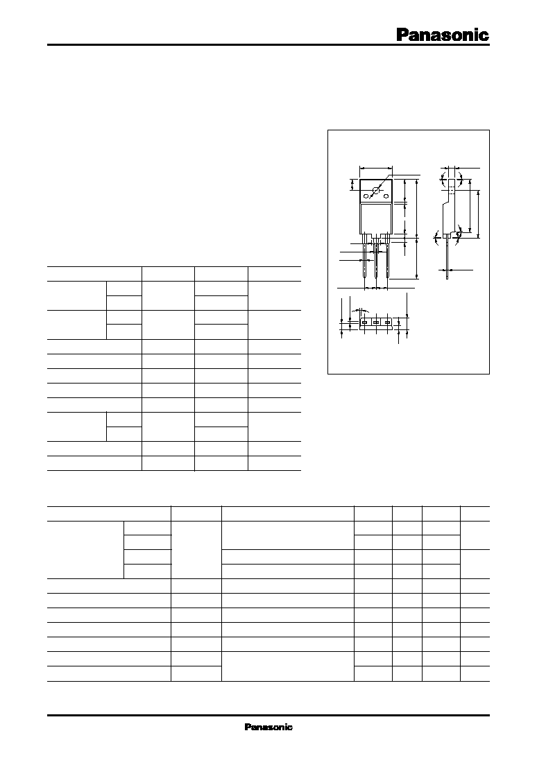
Unit: mm
1:Base
2:Collector
3:Emitter
TOP≠3E Full Pack Package
15.5
±
0.5
26.5
±
0.5
22.0
±
0.5
23.4
18.6
±
0.5
3.3
±
0.3
5.5
±
0.3
2.0
0.7
±
0.1
2.0
2
.0
1.2
10.0
3.0
±
0.3
3.2
±
0.1
4.5
5.45
±
0.3
1
2
3
5.45
±
0.3
1.1
±
0.1
2.0
±
0.2
4.0
5
∞
5
∞
5
∞
5
∞
5
∞
5
∞
0.7
±
0.1
2
Power Transistors
2SC5270, 2SC5270A
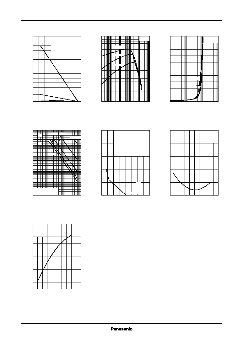
P
C
-- Ta
h
FE
-- I
C
V
CE(sat)
-- I
C
Area of safe operation (ASO)
Area of safe operation, horizontal operation ASO
t
f
-- I
B
t
stg
-- I
B
0
160
40
120
80
140
20
100
60
0
140
120
40
100
80
20
60
(1) T
C
=Ta
(2) With a 100
◊
100
◊
2mm
Al heat sink.
(3) Without heat sink
(P
C
=3.0W)
(1)
(3)
(2)
Ambient temperature Ta (∞C)
Collector power dissipation P
C
(W
)
1
10
5
10
3
10
10
4
10
2
1
10
2
10
V
CE
=5V
T
C
=100∞C
25∞C
≠25∞C
Collector current I
C
(mA)
Forward current transfer ratio h
FE
10
2
10
3
10
4
10
5
0
5000
4000
3000
2000
1000
I
C
/I
B
=4
T
C
=100∞C
25∞C
≠25∞C
Collector current I
C
(mA)
Collector to emitter saturation voltage V
CE(sat)
(V
)
1
10
100
1000
3
30
300
0.001
0.01
0.1
1
100
10
10ms
100ms
1ms
t=100
µ
s
DC
I
CP
I
C
Non repetitive pulse
T
C
=25∞C
Collector to emitter voltage V
CE
(V)
Collector current I
C
(A
)
0
2000
500
1500
1000
0
50
40
30
20
10
f=64kHz, T
C
<90∞C
Area of safe operation with
respect to the single pulse
overload curve at the time of
switching ON, shutting down
by the high voltage spark,
holding down and like that,
during horizontal operation.
<1mA
2SC5270 2SC5270A
Collector to emitter voltage V
CE
(V)
Collector current I
C
(A
)
0
5
4
1
3
2
0
1.0
0.8
0.6
0.4
0.2
0.6
0.7
0.5
0.3
0.1
T
C
=25∞C
I
C
=6A
fH=64kHz
End-of-scan current I
B end
(A)
Switching time t
f
(
µ
s
)
0
5
4
1
3
2
0
10
8
6
4
2
9
7
5
3
1
T
C
=25∞C
I
C
=6A
fH=64kHz
End-of-scan current I
B end
(A)
Switching time t
stg
(
µ
s
)