1
Power Transistors
2SB968
Silicon PNP epitaxial planar type
For low-frequency output amplification
Complementary to 2SD1295
s
Features
q
Possible to solder the radiation fin directly to printed cicuit board
q
High collector to emitter V
CEO
q
Large collector power dissipation P
C
s
Absolute Maximum Ratings
(Ta=25∞C)
Parameter
Collector to base voltage
Collector to emitter voltage
Emitter to base voltage
Peak collector current
Collector current
Collector power dissipation (T
C
=25
∞
C)
Junction temperature
Storage temperature
Symbol
V
CBO
V
CEO
V
EBO
I
CP
I
C
P
C
T
j
T
stg
Ratings
≠50
≠40
≠5
≠3
≠1.5
20
150
≠55 to +150
Unit
V
V
V
A
A
W
∞C
∞C
s
Electrical Characteristics
(T
C
=25∞C)
Parameter
Collector cutoff current
Emitter cutoff current
Collector to base voltage
Collector to emitter voltage
Forward current transfer ratio
Collector to emitter saturation voltage
Base to emitter saturation voltage
Transition frequency
Collector output capacitance
Symbol
I
CBO
I
CEO
I
EBO
V
CBO
V
CEO
h
FE
*
V
CE(sat)
V
BE(sat)
f
T
C
ob
Conditions
V
CB
= ≠20V, I
E
= 0
V
CE
= ≠10V, I
B
= 0
V
EB
= ≠5V, I
C
= 0
I
C
= ≠1mA, I
E
= 0
I
C
= ≠2mA, I
B
= 0
V
CE
= ≠5V, I
C
= ≠1A
I
C
= ≠1.5A, I
B
= ≠ 0.15A
I
C
= ≠2A, I
B
= ≠ 0.2A
V
CB
= ≠5V, I
E
= 0.5A, f = 200MHz
V
CB
= ≠20V, I
E
= 0, f = 1MHz
min
≠50
≠40
50
typ
150
45
max
≠1
≠100
≠10
220
≠1
≠1.5
Unit
µ
A
µ
A
µ
A
V
V
V
V
MHz
pF
*
h
FE
Rank classification
Rank
P
Q
R
h
FE
50 to 100
80 to 160
120 to 220
Unit: mm
1:Base
2:Collector
3:Emitter
U Type Package
6.5
±
0.1
5.3
±
0.1
4.35
±
0.1
4.6
±
0.1
2.3
±
0.1
0.75
±
0.1
1
2
3
0.93
±
0.1
2.5
±
0.1
0.8max
1.0
±
0.2
7.3
±
0.1
1.8
±
0.1
2.3
±
0.1
0.5
±
0.1
0.5
±
0.1
0.1
±
0.05
1.0
±
0.1
6.5
±
0.2
2.3
5.35
4.35
13.3
±
0.3
2.3
±
0.1
5.5
±
0.2
6.0
1.8
0.75
0.6
3
2.3
2
1
0.5
±
0.1
1:Base
2:Collector
3:Emitter
EIAJ:SC≠63
U Type Package (Z)
Unit: mm
2
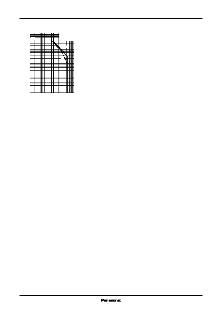
Power Transistors
2SB968
P
C
-- Ta
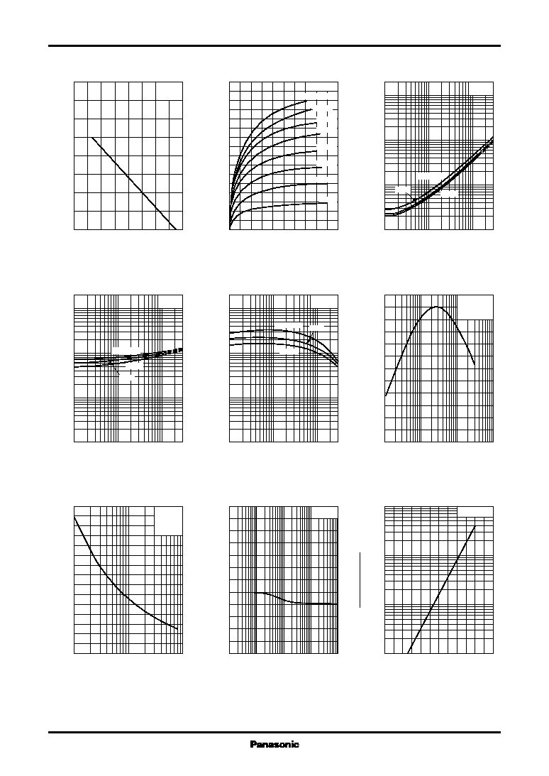
I
C
-- V
CE
V
CE(sat)
-- I
C
V
BE(sat)
-- I
C
h
FE
-- I
C
f
T
-- I
E
C
ob
-- V
CB
V
CER
-- R
BE
I
CEO
-- Ta
0
160
40
120
80
140
20
100
60
0
32
24
8
20
28
16
4
12
T
C
=Ta
Ambient temperature Ta (∞C)
Collector power dissipation P
C
(W
)
0
≠10
≠8
≠2
≠6
≠4
0
≠4.0
≠3.0
≠1.0
≠2.5
≠3.5
≠2.0
≠ 0.5
≠1.5
T
C
=25∞C
I
B
=≠40mA
≠5mA
≠10mA
≠15mA
≠20mA
≠25mA
≠30mA
≠35mA
Collector to emitter voltage V
CE
(V)
Collector current I
C
(A
)
≠ 0.01
≠3
≠1
≠ 0.1
≠ 0.03
≠ 0.3
≠ 0.01
≠ 0.03
≠ 0.1
≠ 0.3
≠1
≠3
≠10
I
C
/I
B
=10
T
C
=100∞C
25∞C
≠25∞C
Collector current I
C
(A)
Collector to emitter saturation voltage V
CE(sat)
(V
)
≠ 0.01
≠3
≠1
≠ 0.1
≠ 0.03
≠ 0.3
≠ 0.01
≠ 0.03
≠ 0.1
≠ 0.3
≠1
≠3
≠10
I
C
/I
B
=10
T
C
=≠25∞C
25∞C
100∞C
Collector current I
C
(A)
Base to emitter saturation voltage V
BE(sat)
(V
)
≠ 0.01
≠3
≠1
≠ 0.1
≠ 0.03
≠ 0.3
1
3
10
30
100
300
1000
V
CE
=≠5V
T
C
=100∞C
25∞C
≠25∞C
Collector current I
C
(A)
Forward current transfer ratio h
FE
10
100
1000
10000
30
300
3000
0
240
200
160
120
80
40
V
CB
=≠5V
f=200MHz
T
C
=25∞C
Emitter current I
E
(mA)
Transition frequency f
T
(MHz
)
≠1
≠3
≠10
≠30
≠100
0
150
120
60
90
30
I
E
=0
f=1MHz
T
C
=25∞C
Collector to base voltage V
CB
(V)
Collector output capacitance C
ob
(pF
)
0.001
0.01
0.1
1
10
0
≠120
≠100
≠80
≠60
≠40
≠20
T
C
=25∞C
Base to emitter resistance R
BE
(k
)
Collector to emitter voltage V
CER
(V
)
0
120
100
80
20
60
40
1
1000
100
10
3
30
300
V
CE
=≠12V
Ambient temperature Ta (∞C)
I
CEO
(Ta
)
I
CEO
(Ta=25∞C
)