
1
Transistor
2SD2067 (Tentative)
Silicon NPN epitaxial planer type
For low-frequency output amplification
s
Features
q
Darlington connection.
q
High foward current transfer ratio h
FE
.
q
Large peak collector current I
CP
.
q
High collector to emitter voltage V
CEO
.
q
Allowing supply with the radial taping.
s
Absolute Maximum Ratings
(Ta=25∞C)
Unit: mm
Parameter
Collector to base voltage
Collector to emitter voltage
Emitter to base voltage
Peak collector current
Collector current
Collector power dissipation
Junction temperature
Storage temperature
1:Emitter
2:Collector
3:Base
MT2 Type Package
2.5
±
0.1
4.5
±
0.1
14.5
±
0.5
2.5
±
0.5
2.5
±
0.5
2.5
±
0.1
6.9
±
0.1
1.05
±
0.05
(1.45)
4.0
0.7
0.8
0.15
0.5
0.2
1.0
1.0
0.65 max.
0.45
+0.1
≠0.05
0.45
+0.1
≠0.05
3
2
1
Symbol
V
CBO
V
CEO
V
EBO
I
CP
I
C
P
C
*
T
j
T
stg
Ratings
120
100
5
3
2
1
150
≠55 ~ +150
Unit
V
V
V
A
A
W
∞C
∞C
s
Electrical Characteristics
(Ta=25∞C)
Parameter
Collector cutoff current
Emitter cutoff current
Collector to base voltage
Collector to emitter voltage
Emitter to base voltage
Forward current transfer ratio
Collector to emitter saturation voltage
Base to emitter saturation voltage
Symbol
I
CBO
I
EBO
V
CBO
V
CEO
V
EBO
h
FE
*1
V
CE(sat)
V
BE(sat)
Conditions
V
CB
= 25V, I
E
= 0
V
EB
= 4V, I
C
= 0
I
C
= 100
µ
A, I
E
= 0
I
C
= 1mA, I
B
= 0
I
E
= 100
µ
A, I
C
= 0
V
CE
= 10V, I
C
= 1A
*2
I
C
= 1A, I
B
= 1mA
*2
I
C
= 1A, I
B
= 1mA
*2
min
120
100
5
4000
typ
max
0.1
1
40000
1.5
2
Unit
µ
A
µ
A
V
V
V
V
V
*1
h
FE
Rank classification
Rank
Q
R
S
h
FE
4000 ~ 10000 8000 ~ 20000 16000 ~ 40000
1.2
±
0.1
0.65
max.
0.45
0.1
0.05
+
≠
Note: In addition to the
lead type shown in
the upper figure, the
type as shown in
the lower figure is
also available.
(HW type)
*2
Pulse measurement
*
Printed circuit board: Copper foil area of 1cm
2
or more, and the board
thickness of 1.7mm for the collector portion
Internal Connection
B
C
E
200
2
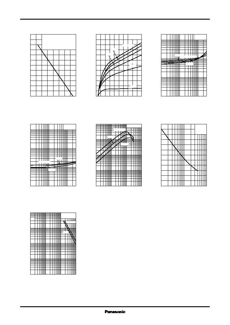
Transistor
2SD2067
P
C
-- Ta
I
C
-- V
CE
V
CE(sat)
-- I
C
V
BE(sat)
-- I
C
h
FE
-- I
C
C
ob
-- V
CB
Area of safe operation (ASO)
0
160
40
120
80
140
20
100
60
0
1.2
1.0
0.8
0.6
0.4
0.2
Printed circut board: Copper
foil area of 1cm
2
or more, and
the board thickness of 1.7mm
for the collector portion.
Ambient temperature Ta (∞C)
Collector power dissipation P
C
(W
)
0
10
8
2
6
4
0
3.0
2.5
2.0
1.5
1.0
0.5
Ta=25∞C
I
B
=180
µ
A
30
µ
A
60
µ
A
90
µ
A
120
µ
A
150
µ
A
Collector to emitter voltage V
CE
(V)
Collector current I
C
(A
)
0.01
3
1
0.1
0.03
0.3
0.01
0.03
0.1
0.3
1
3
10
I
C
/I
B
=1000
Ta=100∞C
25∞C
≠25∞C
Collector current I
C
(A)
Collector to emitter saturation voltage V
CE(sat)
(V
)
0.01
3
1
0.1
0.03
0.3
0.1
0.3
1
3
10
30
100
I
C
/I
B
=1000
Ta=≠25∞C
25∞C
100∞C
Collector current I
C
(A)
Base to emitter saturation voltage V
BE(sat)
(V
)
0.01
0.1
1
10
0.03
0.3
3
10
10
2
10
3
10
4
10
5
V
CE
=10V
Ta=100∞C
25∞C
≠25∞C
Collector current I
C
(A)
Forward current transfer ratio h
FE
1
3
10
30
100
0
60
50
40
30
20
10
I
E
=0
f=1MHz
Ta=25∞C
Collector to base voltage V
CB
(V)
Collector output capacitance C
ob
(pF
)
0.1
1
10
100
0.3
3
30
0.001
0.003
0.01
0.03
0.1
0.3
1
3
10
Single pulse
Ta=25∞C
t=10ms
t=1s
I
CP
I
C
Collector to emitter voltage V
CE
(V)
Collector current I
C
(A
)