1
Power Transistors
2SD2215, 2SD2215A
Silicon NPN triple diffusion planar type
For power amplification
s
Features
q
High collector to base voltage V
CBO
q
I type package enabling direct soldering of the radiating fin to
the printed circuit board, etc. of small electronic equipment.
s
Absolute Maximum Ratings
(T
C
=25∞C)
Parameter
Collector to
base voltage
Collector to
emitter voltage
Emitter to base voltage
Peak collector current
Collector current
Collector power
dissipation
Junction temperature
Storage temperature
Symbol
V
CBO
V
CEO
V
EBO
I
CP
I
C
P
C
T
j
T
stg
Ratings
350
400
250
300
5
1.5
0.75
15
1.3
150
≠55 to +150
Unit
V
V
V
A
A
W
∞C
∞C
2SD2215
2SD2215A
2SD2215
2SD2215A
T
C
=25
∞
C
Ta=25
∞
C
s
Electrical Characteristics
(T
C
=25∞C)
Parameter
Collector cutoff
current
Collector cutoff
current
Emitter cutoff current
Collector to emitter
voltage
Forward current transfer ratio
Base to emitter voltage
Collector to emitter saturation voltage
Transition frequency
Turn-on time
Storage time
Fall time
Symbol
I
CES
I
CEO
I
EBO
V
CEO
h
FE1
*
h
FE2
V
BE
V
CE(sat)
f
T
t
on
t
stg
t
f
Conditions
V
CE
= 350V, V
BE
= 0
V
CE
= 400V, V
BE
= 0
V
CE
= 150V, I
B
= 0
V
CE
= 200V, I
B
= 0
V
EB
= 5V, I
C
= 0
I
C
= 30mA, I
B
= 0
V
CE
= 10V, I
C
= 0.3A
V
CE
= 10V, I
C
= 1A
V
CE
= 10V, I
C
= 1A
I
C
= 1A, I
B
= 0.2A
V
CE
= 5V, I
C
= 0.5A, f = 10MHz
I
C
= 1A, I
B1
= 0.1A, I
B2
= ≠ 0.1A,
V
CC
= 50V
min
250
300
70
10
typ
30
0.5
2
0.5
max
1
1
1
1
1
250
1.5
1
Unit
mA
mA
mA
V
V
V
MHz
µ
s
µ
s
µ
s
2SD2215
2SD2215A
2SD2215
2SD2215A
2SD2215
2SD2215A
*
h
FE1
Rank classification
Rank
Q
P
h
FE1
70 to 150
120 to 250
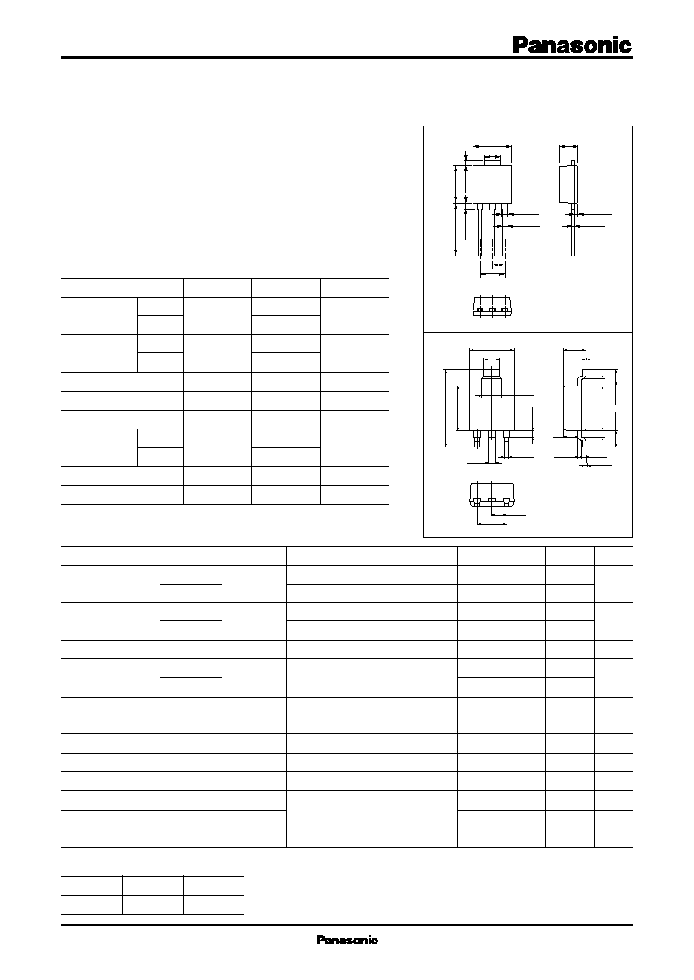
Unit: mm
1:Base
2:Collector
3:Emitter
I Type Package
Unit: mm
1:Base
2:Collector
3:Emitter
I Type Package (Y)
7.2
±
0.3
7.0
±
0.3
3.0
±
0.2
3.5
±
0.2
10.0
+0.3
≠0.
0.8
±
0.2
1.0
±
0.2
4.6
±
0.4
2
1
3
1.1
±
0.1
0.75
±
0.1
2.3
±
0.2
0.85
±
0.1
0.4
±
0.1
7.0
±
0.3
0.75
±
0.1
2.3
±
0.2
4.6
±
0.4
1.1
±
0.1
10.2
±
0.3
7.2
±
0.3
2.0
±
0.2
0.9
±
0.1
3.5
±
0.2
2.5
±
0.2
1.0
1.0
2.5
±
0.2
3.0
±
0.2
1.0 max.
1
2
3
0 to 0.15
0 to 0.15
2.5
0.5 max.
2
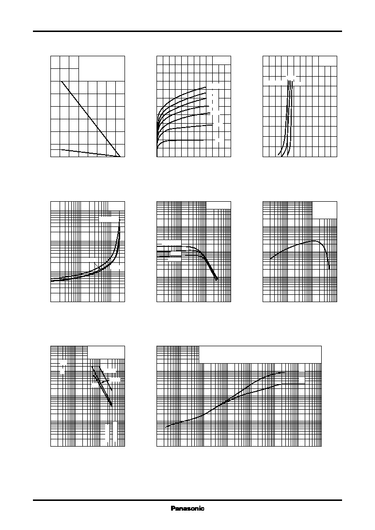
Power Transistors
2SD2215, 2SD2215A
P
C
-- Ta
I
C
-- V
CE
I
C
-- V
BE
V
CE(sat)
-- I
C
h
FE
-- I
C
f
T
-- I
C
Area of safe operation (ASO)
R
th(t)
-- t
0
160
40
120
80
140
20
100
60
0
20
15
5
10
(1) T
C
=Ta
(2) Without heat sink
(P
C
=1.3W)
(1)
(2)
Ambient temperature Ta (∞C)
Collector power dissipation P
C
(W
)
0
12
10
8
2
6
4
0
1.2
1.0
0.8
0.6
0.4
0.2
I
B
=14mA
12mA
10mA
2mA
4mA
6mA
8mA
T
C
=25∞C
Collector to emitter voltage V
CE
(V)
Collector current I
C
(A
)
0
2.4
2.0
1.6
0.4
1.2
0.8
0
4.0
3.2
2.4
1.6
0.8
T
C
=100∞C
25∞C
≠25∞C
V
CE
=10V
Base to emitter voltage V
BE
(V)
Collector current I
C
(A
)
0.01
3
1
0.1
0.03
0.3
0.01
0.03
0.1
0.3
1
3
10
I
C
/I
B
=10
T
C
=100∞C
25∞C
≠25∞C
Collector current I
C
(A)
Collector to emitter saturation voltage V
CE(sat)
(V
)
0.01
0.1
1
10
0.03
0.3
3
1
3
10
30
100
300
1000
3000
10000
V
CE
=10V
T
C
=100∞C
25∞C
≠25∞C
Collector current I
C
(A)
Forward current transfer ratio h
FE
0.001
0.01
0.1
1
0.003
0.03
0.3
0.1
0.3
1
3
10
30
100
300
1000
V
CE
=10V
f=10MHz
T
C
=25∞C
Collector current I
C
(A)
Transition frequency f
T
(MHz
)
1
10
100
1000
3
30
300
0.001
0.003
0.01
0.03
0.1
0.3
1
3
10
10ms
t=1ms
DC
2SD2215
2SD2215A
I
CP
I
C
Non repetitive pulse
T
C
=25∞C
Collector to emitter voltage V
CE
(V)
Collector current I
C
(A
)
10
≠3
10
2
10
≠2
1
10
≠1
10
10
3
10
4
0.1
1
10
100
1000
Note: R
th
was measured at Ta=25∞C and under natural convection.
(1) Without heat sink
(2) With a 50
◊
50
◊
2mm Al heat sink
(1)
(2)
Time t (s)
Thermal resistance R
th
(t)
(∞C/W
)