1
Power Transistors
2SD2528
Silicon NPN epitaxial planar type
For power amplification with high forward current transfer ratio
s
Features
q
High foward current transfer ratio h
FE
q
Satisfactory linearity of foward current transfer ratio h
FE
q
Full-pack package which can be installed to the heat sink with
one screw
s
Absolute Maximum Ratings
(T
C
=25∞C)
Parameter
Collector to base voltage
Collector to emitter voltage
Emitter to base voltage
Peak collector current
Collector current
Base current
Collector power
dissipation
Junction temperature
Storage temperature
Symbol
V
CBO
V
CEO
V
EBO
I
CP
I
C
I
B
P
C
T
j
T
stg
Ratings
80
60
6
10
5
1
40
2.0
150
≠55 to +150
Unit
V
V
V
A
A
A
W
∞C
∞C
s
Electrical Characteristics
(T
C
=25∞C)
Parameter
Collector cutoff current
Emitter cutoff current
Collector to emitter voltage
Forward current transfer ratio
Collector to emitter saturation voltage
Transition frequency
Turn-on time
Storage time
Fall time
Symbol
I
CBO
I
EBO
V
CEO
h
FE
*
V
CE(sat)
f
T
t
on
t
stg
t
f
Conditions
V
CB
= 80V, I
E
= 0
V
EB
= 6V, I
C
= 0
I
C
= 25mA, I
B
= 0
V
CE
= 4V, I
C
= 1A
I
C
= 4A, I
B
= 0.1A
V
CE
= 12V, I
C
= 0.4A, f = 10MHz
I
C
= 4A, I
B1
= 0.08A, I
B2
= ≠ 0.08A,
V
CC
= 50V
min
60
500
typ
30
0.4
2.0
0.6
max
100
100
2000
0.3
Unit
µ
A
µ
A
V
V
MHz
µ
s
µ
s
µ
s
*
h
FE
Rank classification
Rank
P
Q
h
FE
800 to 2000 500 to 1200
T
C
=25
∞
C
Ta=25
∞
C
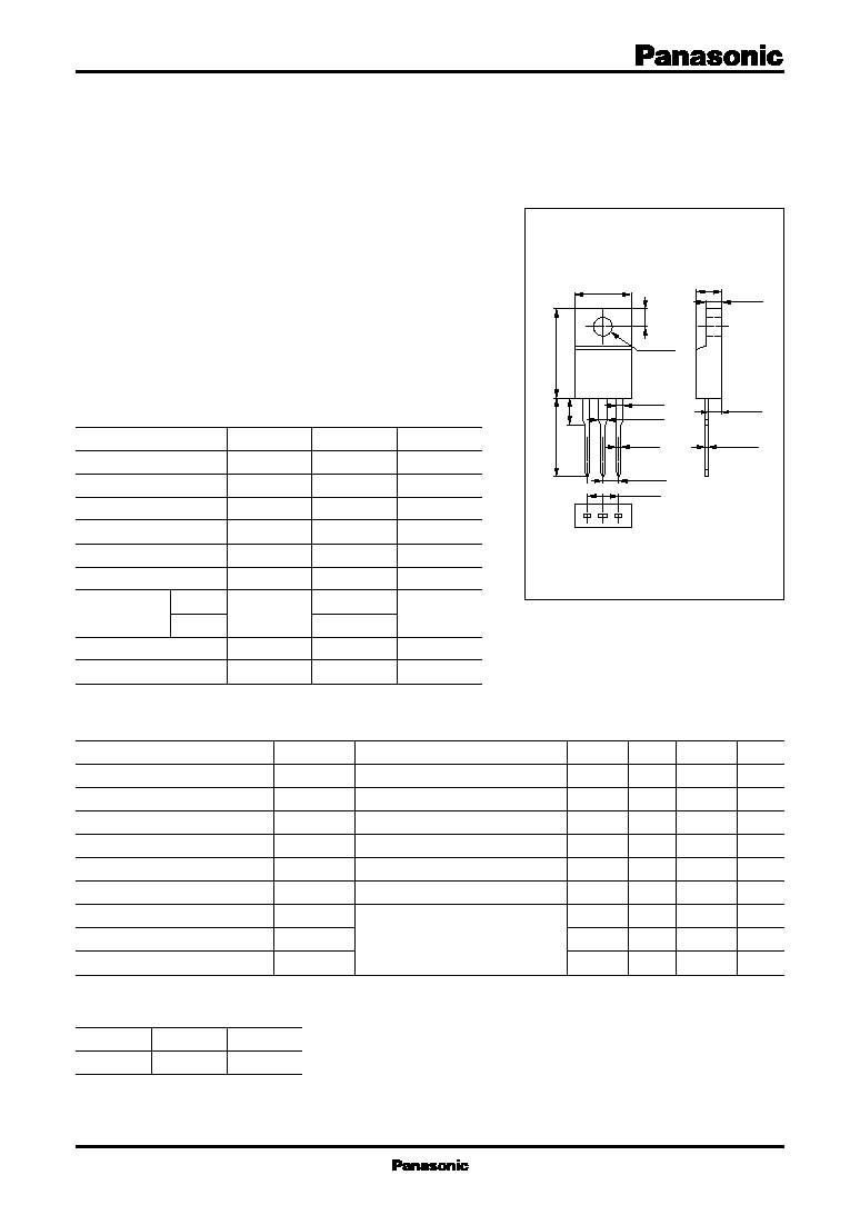
Unit: mm
1:Base
2:Collector
3:Emitter
TO≠220D Full Pack Package
1
9.9
±
0.3
15.0
±
0.5
13.7
±
0.2
4.2
±
0.2
4.6
±
0.2
2.9
±
0.2
0.8
±
0.1
1.4
±
0.2
2
3
3.2
±
0.1
2.6
±
0.1
0.55
±
0.15
2.54
±
0.3
5.08
±
0.5
3.0
±
0.5
1.6
±
0.2
2
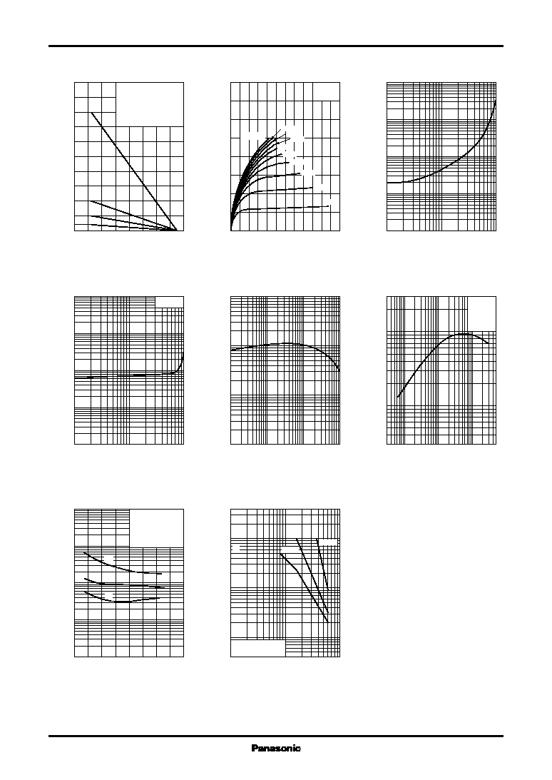
Power Transistors
2SD2528
P
C
-- Ta
I
C
-- V
CE
V
CE(sat)
-- I
C
V
BE(sat)
-- I
C
h
FE
-- I
C
f
T
-- I
C
t
on
, t
stg
, t
f
-- I
C
Area of safe operation (ASO)
0
160
40
120
80
140
20
100
60
0
50
40
30
20
10
(1) T
C
=Ta
(2) With a 100
◊
100
◊
2mm
Al heat sink
(3) With a 50
◊
50
◊
2mm
Al heat sink
(4) Without heat sink
(1)
(2)
(3)
(4)
Ambient temperature Ta (∞C)
Collector power dissipation P
C
(W
)
0
12
10
8
2
6
4
0
8
6
2
5
7
4
1
3
T
C
=25∞C
I
B
=10mA
9mA
8mA
7mA
6mA
5mA
4mA
3mA
2mA
1mA
Collector to emitter voltage V
CE
(V)
Collector current I
C
(A
)
10
≠1
1
10
10
≠3
10
≠2
10
≠1
1
10
Collector current I
C
(A)
Collector to emitter saturation voltage V
CE(sat)
(V
)
10
≠1
1
10
10
≠2
10
≠1
1
10
10
2
I
C
/I
B
=50
Collector current I
C
(A)
Base to emitter saturation voltage V
BE(sat)
(V
)
10
≠2
10
≠1
1
10
10
10
4
10
3
10
2
Collector current I
C
(A)
Forward current transfer ratio h
FE
0.003
0.1
0.01
0.3
0.03
1
3
100
10
30
3
300
V
CE
=12V
f=10MHz
T
C
=25∞C
Collector current I
C
(A)
Transition frequency f
T
(MHz
)
0
8
2
6
4
7
1
5
3
0.01
0.03
0.1
0.3
1
3
10
30
100
Pulsed t
w
=1ms
Duty cycle=1%
I
C
/I
B
=50 (I
B1
=≠I
B2
)
V
CC
=50V
T
C
=25∞C
t
stg
t
f
t
on
Collector current I
C
(A)
Switching time t
on
,t
stg
,t
f
(
µ
s
)
1
3
10
30
100
10
30
1
0.1
0.3
3
Non repetitive pulse
T
C
=25∞C
I
CP
I
C
10ms
1s
t=1ms
Collector to emitter voltage V
CE
(V)
Collector current I
C
(A
)