ICs for VCR
1
AN2493FH
Luminance and chrominance signal processing (PAL) IC
for 8 mm VCR
s
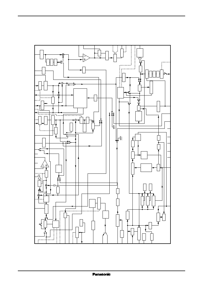
Overview
The AN2493FH is a single chip LSI designed for a Y/
C main signal processing of PAL system normal 8 mm
video. System cost can be cut down drastically by built-
in of external filters and fc automatic adjustment.
s
Features
∑
5 V single power supply
∑
Reduction of external components and adjustment parts
by adopting of automatic adjustment filters.
∑
No need of glass delay lines.
s
Applications
∑
8 mm videos and 8 mm video cameras
QFP064-P-1010
Unit: mm
10.00
±
0.20
48
33
32
17
16
1
64
49
12.00
±
0.20
10.00
±
0.20
0.10
±
0.10
12.00
±
0.20
1.95
±
0.20
(1.25)
(1.25)
0.50
0.18
+
0.10
-
0.05
0.15
+
0.10
-
0.05
Seating plane
(1.00)
0.50
±
0.20
0
∞
to 10
∞
AN2493FH
ICs for VCR
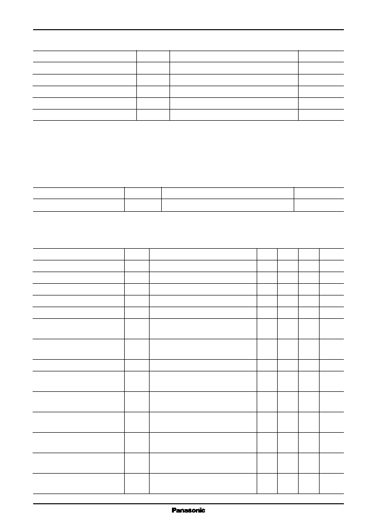
4
Parameter
Symbol
Conditions
Min
Typ
Max
Unit
Consumption current 1
I
CC1
Consumption current at recording
52
72
92
mA
Consumption current 2
I
CC2
Consumption current at playback
58
78
98
mA
Consumption current 3
I
CC3
Power save mode
42
62
82
mA
Consumption current 4
I
CC4
Camera power save mode
-
8
-
4.2
-
1
mA
Internal reference voltage source
V
REF
Pin 3 voltage
2.5
V
REC overall
V
ME
Adjust pin 47 output voltage to
-
14
-
12
-
10
dB
1 V[p-p] at pin 53
Y-AGC control characteristics
V
AGC
Pin 47 output gain ratio between
-
1.5
0
1.5
dB
0.5 V[p-p] and 2.0 V[p-p] inputs
Y-AGC through mode
V
26S
Pin 24 output at pin 50 input
200
250
300
mV[p-p]
View finder amp.
f
BA
Output ratio of 5 MHz to 100 kHz
-
1.5
0
1.5
dB
frequency characteristics
at input of 100 kHz or 5 MHz
Video-OSD
V
OW
DC voltage referred to pedestal level
56
68
80
IRE
white mute level
Video-OSD
V
OB
DC voltage referred to pedestal level
-
5
5
15
IRE
black mute level
Video-OSD
V
48W
Pin 48 input at inserting recording
3.6
4.8
V
white mute CTL voltage
character
Video-OSD
V
48B
Pin 48 input at inserting recording
2.0
2.6
V
black mute CTL voltage
character
Video-OSD
V
48S
Pin 48 input at inserting recording
0
1.0
V
through CTL voltage
character
s
Absolute Maximum Ratings
Parameter
Symbol
Range
Unit
Supply voltage
V
CC
4.7 to 5.2
V
s
Recommended Operating Range
Parameter
Symbol
Rating
Unit
Supply voltage
V
CC
5.5
V
Supply current
I
CC
100
mA
Power dissipation
*2
P
D
359
mW
Operating ambient temperature
*1,
*3
T
opr
-
10 to
+
70
∞
C
Storage temperature
*1
T
stg
-
55 to
+
125
∞
C
Note) *1: Except for the power dissipation, operating ambient temperature and storage temperature, all ratings are for T
a
=
25
∞
C.
*2: The power dissipation shown is for the IC package at T
a
=
70
∞
C.
P
D
=
696 (mW) (T
a
=
70∞C) when mounted on the glass epoxy printed circuit board of 50
◊
50
◊
0.8 (mm
3
).
*3: It becomes
=
471(mW) at supply voltage V
CC
=
4.8 V.
s
Electrical Characteristics at V
CC
=
4.8 V, T
a
=
25
∞
C
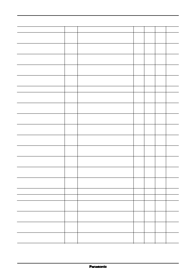
ICs for VCR
AN2493FH
5
Parameter
Symbol
Conditions
Min
Typ
Max
Unit
Video-OSD quasi-V level
V
OV
DC voltage difference referred to
-
50
0
50
mV
sync. tip in PB mode
Video-OSD quasi-V
V
48V
Pin 48 input in PB mode
2.0
4.8
V
mute CTL voltage
Video-OSD
V
48G
Pin 48 input in PB mode
0
1.0
V
through CTL voltage
Y-main-LPF
f
ML1
Output ratio of 3 MHz to 100 kHz
-
5
-
1
2
dB
frequency characteristics 1
at input of 100 kHz or 3 MHz
Y-main-LPF
f
ML2
Output ratio of 4.43 MHz to 100 kHz
-
25
dB
frequency characteristics 2
at input of 100 kHz or 4.43 MHz
Video amp. output amplitude
V
VO
Adjust the VF out to 1 V[p-p]
1.75
2.0
2.25
V[p-p]
Video amp.
f
VI
Output ratio of 5 MHz to 100 kHz
-
1.5
0
1.5
dB
frequency characteristics
at input of 100 kHz or 5 MHz
View finder OSD-white
V
BOW
DC voltage referred to pedestal level
56
68
80
IRE
mute level
View finder OSD-black
V
BOB
DC voltage referred to pedestal level
-
5
5
15
IRE
mute level
View finder OSD-white
V
46W
Pin 48
=
0 V, an indication character
3.6
4.8
V
mute CTL voltage
is inserted
View finder OSD-black
V
46B
Pin 48
=
0 V, an indication character
2.0
2.6
V
mute CTL voltage
is inserted
View finder OSD
V
46S
Pin 48
=
0 V, an indication character
0
1.0
V
through CTL voltage
is inserted
View finder OSD quasi-V level
V
BOV
DC voltage referred to sync. tip at
-
50
0
50
mV
PB mode
View finder OSD quasi-V
V
B48V
Pin 48 input in PB mode
2.0
4.8
V
mute CTL voltage
View finder OSD
V
B48S
Pin 48 input in PB mode
0
1.0
V
through CTL voltage
PB OSD white mute level
V
POW
DC voltage referred to pedestal level
56
68
80
IRE
PB OSD black mute level
V
POB
DC voltage referred to pedestal level
-
5
5
15
IRE
PB OSD white
V
46W
Pin 48
=
0 V, an indication character
3.6
4.8
V
mute CTL voltage
is inserted
PB OSD black
V
46B
Pin 48
=
0 V, an indication character
2.0
2.6
V
mute CTL voltage
is inserted
PB OSD through CTL voltage
V
46S
Pin 48
=
0 V, an indication character
0
1.0
V
is inserted
PB OSD off
V
VOO
Pin 48
=
0 V, an indication character
1.75
2.0
2.25
V[p-p]
is inserted
s
Electrical Characteristics at T
a
=
25
∞
C (continued)