 | –≠–ª–µ–∫—Ç—Ä–æ–Ω–Ω—ã–π –∫–æ–º–ø–æ–Ω–µ–Ω—Ç: AN3986FHP | –°–∫–∞—á–∞—Ç—å:  PDF PDF  ZIP ZIP |

1
ICs for Video Camera
s
Overview
The AN3986FBP and the AN3986FHP are stereo audio
signal processor ICs for 8-mm camcorder. It incorporates
all the functions needed for stereo-audio signal process-
ing in 8mm camcorder.
s
Features
∑
Built-in headphone amplifiers
∑
Built-in matrix signal processing
AN3986FBP, AN3986FHP
Stereo Audio Signal Processor ICs for 8-mm Camcorder
Supply voltage
Power dissipation
Note 2)
Operating ambient temperature
Note 1)
Storage temperature
Note 1)
V
CC
P
D
T
opr
T
stg
V
CC1
=6 / V
CC2
=9.5
392
≠20 to + 70
≠55 to + 125
V
mW
∞C
∞C
Parameter
Symbol
Rating
Unit
Note 1) Ta=25∞C except operating ambient temperature and storage temperature unless otherwise specified.
Note 2) Allowable power dissipation of the package at Ta=70∞C.
AN3986FHP
Supply voltage
Power dissipation
Note 2)
Operating ambient temperature
Note 1)
Storage temperature
Note 1)
V
CC
P
D
T
opr
T
stg
V
CC1
= 6 / V
CC2
= 9.5
474
≠ 20 to + 70
≠ 55 to + 125
V
mW
∞C
∞C
Parameter
Symbol
Rating
Unit
s
Absolute Maximum Ratings
AN3986FBP
Unit : mm
21.2
±
0.2
18.0
±
0.2
3.3max.
1.55
±
0.1
1.55
±
0.1
0.15
+ 0.1
≠ 0.05
21
1
22
18.0
±
0.2
21.2
±
0.2
0.1
(0.6)
3.4
+ 0.15
≠ 0.3
0.1
±
0.1
0.8
0.35
+ 0.1
≠ 0.05
42
43
63
64
84
AN3986FBP
84-Pin QFH Package (QFH084-P-1818)
Unit : mm
80-Pin QFH Package (QFH080-P-1212)
12.0
±
0.2
14.0
±
0.2
12.0
±
0.2
14.00.2
(0.5)
(min0.25)
1.3
±
0.1
1.3
±
0.1
2.8
±
0.2
0.15
≠ 0.05
+ 0.1
0.1
±
0.1
0.5
0.2
1
AN3986FHP
2
ICs for Video Camera
AN3986FBP, AN3986FHP
+
10
µ
F
10
µ
F
+
2.2
µ
F
0.01
µ
F
50k
VR
10k
5.6k
4.7
µ
F
47
µ
F4
.
7
µ
F
4700pF
4700pF
+
4.7
µ
F
+
4.7
µ
F
100
µ
F
+
4.7
µ
F
0.01
µ
F
+
1
µ
F
+
4.7
µ
F
10
µ
F
65
41
22
40
39
38
37
36
35
34
33
32
31
30
29
28
27
26
25
24
23
44
45
46
47
48
49
50
51
52
53
54
55
56
57
58
59
60
61
62
63
20
19
18
17
16
15
14
13
12
11
10
9
8
7
6
5
4
3
2
1
V
CC
Rch
Output
Convert
+
6.8k
0.01
µ
F
0.01
µ
F
BPF
1
µ
F
0.01
µ
F
0.01
µ
F
0.01
µ
F
0.047
µ
F
ST
MONO
BIL
ST
to Control
to Control
to FMOUT
330pF
0.01
µ
F
33k
MM
+
MUTE
8.2k
0.01
µ
F
BPF
0.01
µ
F
LIM
LPF
HOLD
PC
VCO
AL
+
10
µ
F
+
≠
10
µ
F
+
2.2
µ
F
0.01
µ
F
≠
+
≠
+
≠
+
LP empha
R
+
≠
R
LS
CCA
50k
VR
10k
5.6k
4700pF
4.7
µ
F
+
47
µ
F4
.
7
µ
F
LFP
4700pF
4700pF
R
R
R
R
R
RR
Matrix
to Control
+
4.7
µ
F
AGC
Fade
LPF
LPF
Vo1
+
47
µ
F
V
REF
+
100
µ
F
+
+
4.7
µ
F
+
47
µ
F
V
REFH
+
100
µ
F
0.01
µ
F
4.7
µ
F
+
+
100
µ
F
0.01
µ
F
+
+
4.7
µ
F
10k
VR
R
V
CCH
4700pF
+
+
Control
VCO Adjust (R)
FMOUT
(R)
ST/MONO Time constant
HOLD 1
HOLD 2
Timing making
PG GND
PG Input
MUTE Time constant
MUTE detection
FMOUT (L)
VCO Adjuse (R)
0.01
µ
F
Input 3 (R)
HP Vol Control
Input 2 (R)
Input 1 (R)
V
CC
(4.75V)
HP Output (R)
HP GND (R)
Line Output (R)
V
CCH
(8.2V)
V
REFH
Line Output (L)
HP GND (L)
HP Output (L)
V
REF
Input 1 (L)
AGC Time Constant
Input 2 (L)
Input 3 (L)
PB/Rec Change (PB )
H
Fade Control
R
43
21
64
42
R
+
M
U
T
E
1
/
2
/
3
H
G
N
D
Bil
MONO
ST
I
O
Detect Output
Input
change
S
P
L / R / ST
ON
Auto
OFF
H
G
N
D
I
O
Output
change
Matrix
Control
to Pin37
1
2
3
4
5
6
7
8
9
10
11
12
13
14
15
17
18
19
20
16
21
22
23
24
25
26
27
28
29
30
31
32
33
34
35
36
37
38
39
40
41
42
43
44
45
46
47
48
49
50
51
52
53
54
55
56
57
58
59
60
61
66
62
63
64
65
66
67
68
69
70
71
72
73
74
75
76
77
78
79
80
84
77
78
79
80
81
82
83
67
68
69
70
71
72
73
74
75
76
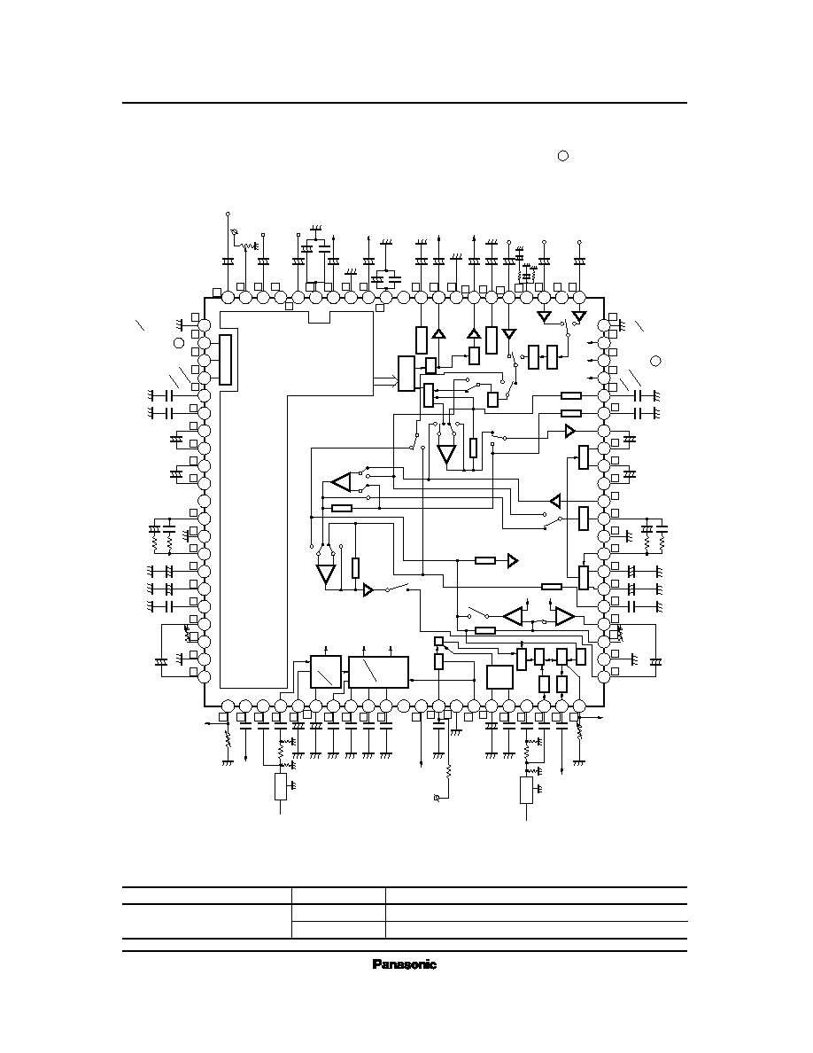
Note) A number with a circle denotes a pin
No. of the AN3986FBP, while a
number with a square denotes a pin
No. of the AN3986FHP.
s
Block Diagram
Parameter
Symbol
Range
Operating supply voltage range
V
CC1
V
CC2
4.5V to 5.5V
4.5V to 9.0V
s
Recommended Operating Range
(Ta=25∞C)

3
ICs for Video Camera
AN3986FBP, AN3986FHP
Pin No.
Pin name
Pin No.
Pin name
43
44
45
46
47
48
49
50
51
52
54
55
56
57
58
59
60
61
62
63
64
65
66
67
68
69
70
71
72
73
75
76
77
78
79
80
81
82
83
84
NR input/output
GND
Dev. adjustment 1
Dev. adjustment 2
LP emphasis
Level sensor timing C1
Level sensor timing C2
Level sensor input
GND
LPF output
CCA amp. input
CCA output
CCA input
Buffer output
FM emphasis
NR emphasis
Mode discriminator output
Mute control
Input change switch
GND
Input 3
Rec/PB switching
Input 2
AGC time-constant
Input 1
V
REF
Headphone output
Headphone GND
Line output
V
REF
H
V
CC2
Line output
Headphone GND
Headphone output
V
CC1
Input 1
Fade control
Input 2
Headphone volume control
Input 3
GND
SP/EP mode switching
Output switching control
Matrix control
NR emphasis
FM emphasis
Buffer input
CCA input
CCA output
CCA amp. input
LPF output
GND
Level sensor input
Level sensor timing C2
Level sensor timing C1
LP emphasis
Dev. adjustment 2
Dev. adjustment 1
GND
NR input/output
VCO frequency adjustment
FM modulator output
FM demodulator input
FM detector input
FM input AGC detection
ST/MON time-constant
HOLD 2
HOLD 1
ST/MON detection
Bilingual timing generation
V
CC1
(FM)
Mono/multi time-constant
GND (PG)
PG input
MUTE time-constant
MUTE detection
FM detection input
FM demodulator input
FM modulator output
VCO frequency adjustment
s
Pin Descriptions
(L)
(L)
(L)
(L)
(L)
(L)
(L)
(L)
(L)
(L)
(L)
(L)
(L)
(L)
(L)
(L)
(L)
(L)
(L)
(L)
(L)
(R)
(R)
(R)
(R)
(R)
(R)
(R)
(R)
(R)
(R)
(R)
(R)
(R)
(R)
(R)
(R)
(R)
(R)
(R)
(R)
(R)
(R)
(R)
(R)
(L)
(L)
(L)
(L)
1
2
3
4
5
6
7
8
9
10
11
12
13
14
15
16
17
18
19
20
21
22
23
24
25
26
27
28
29
30
31
32
33
34
35
36
37
38
39
40
41
42
43
44
45
46
47
48
49
50
51
52
53
54
55
56
57
58
59
60
61
62
63
64
65
66
67
68
69
70
71
72
73
74
75
76
77
78
79
80
AN3986FHP AN3986FBP
AN3986FHP AN3986FBP
1
2
3
4
5
6
7
8
9
10
12
13
14
15
16
17
18
19
20
21
22
23
24
25
26
27
28
29
30
31
33
34
35
36
37
38
39
40
41
42
Note) Pins11, 32, 53, and 74 of the AN3986FBP are to be left open.

4
ICs for Video Camera
AN3986FBP, AN3986FHP
Parameter
Symbol
Condition min
typ
max
Unit
I
R35
Circuit current 1 at recording
58
73
88
mA
I
R31
Circuit current 2 at recording
1.6
2.4
mA
I
P35
Circuit current 1 at playing back
61
93
mA
2.0
77
I
R31
Circuit current 1 at playing back
1.6
2.4
mA
2.0
Line AGC output level Lch, Rch
V
OALL
V
OALR
≠ 8
≠ 7
≠ 6
dBs
Line AGC output distortion factor Lch, Rch
T
HALL1
T
HALR1
0.02
0.1
%
AGC ON output level Lch, Rch
V
OALL2
V
OALR2
≠ 4
≠ 1
+ 2
dBs
AGC ON output distortion factor Lch, Rch
T
HALL2
T
HALR2
0.2
0.4
%
Line AGC output noise Lch, Rch
V
NALL
V
NALR
≠ 78
≠ 74
dBs
Fade control maximum attenuation
output Lch, Rch
V
FALL
V
FALR
≠ 80
≠ 75
dBs
Line through monitor output level
Lch, Rch
V
O1LL
V
O1LR
≠ 8
≠ 7
≠ 6
dBs
Line through monitor output noise
Lch, Rch
V
NLLL
V
NLLR
≠ 81
≠ 77
dBs
Between inputs between channels
crosstalk
≠ 78
≠ 74
dB
V
CTIN
E-E monitor output frequency
characteristics Lch, Rch
V
OLFL
V
OLFR
≠ 5.5
≠ 2.5
dBs
HP output level V
OL
= CENTER
Lch, Rch
V
HC8L
V
HC8R
≠ 28
≠ 26
≠ 24
dBs
HP output distortion factor
V
OL
= CENTER Lch, Rch
T
HHC8L
T
HHC8R
0.05
0.5
%
HP output level V
OL
= MAX Lch, Rch
V
HH8L
V
HH8R
≠ 18
≠ 16
≠ 14
dBs
HP output level V
OL
= MIN Lch, Rch
V
HL8L
V
HL8R
≠ 96
≠ 92
dBs
HP output noise voltage V
OL
= MIN
Lch, Rch
V
NHCOL
V
NHCOR
≠ 96
≠ 92
dBs
HP maximum output level
V
OL
= CENTER Lch, Rch
V
MHH8L
V
MHH8R
≠ 18
dBs
≠ 18
≠ 15
≠ 12
dBs
0.4
%
≠ 21
≠ 19
dB
0.2
≠ 20
3.8
5.8
dB
4.8
LP encode f characteristics Lch, Rch
V
FLRLL
V
FLRLR
2.0
3.0
4.0
dB
Encode output noise Lch, Rch
V
NRRL
V
NRRR
≠ 55
≠ 51
dB
ST/BIL level difference L + R Lch
≠ 0.5
0
+ 0.5
dB
ST/BIL level difference L ≠ R Lch
≠ 30
≠ 17.5
dB
Encode output level Lch, Rch
Encode output distortion factor Lch, Rch
Encode linearity Lch, Rch
SP encode f characteristics Lch, Rch
V
BSRLR
V
BSRLL
V
FORLL
V
FORLR
V
OXLL
V
OXLR
T
HORLL
T
HORLR
V
ORLL
V
ORLR
MON/BIL level difference Lch
≠ 0.5
0
+ 0.5
dB
Decode reference output level Lch, Rch
V
OLPL
V
OLPR
≠ 9.5
≠ 7
≠ 4.5
dB
V
CC1
= 4.75V, when no signal input
V
CC2
= 8.20V, when no signal input
V
CC1
= 4.75V, when no signal input
V
CC2
= 8.20V, when no signal input
V
IN
= 20dBs
f= 400Hz
V
IN
= 20dBs
f= 1kHz, THD 5th
V
IN
= ≠ 2dBs
f= 400Hz
V
IN
= ≠ 2dBs
f= 1kHz, THD 5th
No input A curve filter
No input A curve filter
V
IN
= ≠ 20dBs, 1kHz
A curve filter
No input A curve filter
V
IN
= ≠ 20dBs, 400Hz
V
IN
= ≠14dBs, 1kHz
A curve filter
V
IN
= ≠ 20dBs
ratio of 40kHz/40Hz
V
IN
= ≠ 20dBs, 400Hz
8
load
V
IN
= ≠ 20dBs, 1kHz
8
load, THD 5th
V
IN
= ≠ 20dBs, 400Hz
8
load
V
IN
= ≠ 20dBs, 400Hz
8
load
1kHz, at 1% distortion,
8
load THD 5th
V
IN
= ≠ 20dBs, 400Hz
BIL mode
V
IN
= ≠ 20dBs, 1kHz
to THD 5th
V
IN
= ≠ 11.2/≠51.2BS
f= 400Hz
V
IN
= ≠ 20dBs
f= 10kHz/400Hz
V
IN
= ≠ 20dBs, 10kHz
ratio of LP/SP
No input A curve filter
V
IN
= ≠ 20dBs, 400Hz
V
IN
= ≠ 20dBs, 400Hz
30kHz LPF
V
IN
= ≠ 20dBs, 400Hz
V
OLL
, input V
ORLR
V
BMRLL
s
Electrical Characteristics (cont.)
(V
CC1
= 4.75V, V
CC2
= 8.2V, Ta= 25
±
2∞C)
(AN3986FHP)

5
ICs for Video Camera
AN3986FBP, AN3986FHP
s
Electrical Characteristics (cont.)
(V
CC1
= 4.75V, V
CC2
= 8.2V, Ta= 25
±
2∞C)
(AN3986FHP)
Decode reference output distortion
factor Lch, Rch
T
HOLPL
T
HOLPR
0.12
0.3
%
Decode linearity Lch, Rch
V
OXPL
V
OXPR
≠ 63
≠ 60
≠ 57
dB
Decode output noise Lch, Rch
≠ 87
≠ 79
dBs
Crosstalk Lch, Rch, at playback
C
ERL
C
ERR
≠ 79
dBs
Maximum output level Lch, Rch,
at playback
V
OLML
V
OLMR
0.4
1.0
%
Line mute attenuation quantity Lch, Rch
V
MLML
V
MLMR
≠ 92
≠ 87
dBs
Encode channel crosstalk Lch, Rch
S
ERL
S
ERR
≠ 50
≠ 47
dBs
E≠E system monitor output channel
balance
≠ 0.55
0
+ 0.55
dB
Encode output channel balance
Decode output channel balance
VCO free-run frequency Lch
VCO free-run frequency Rch
VCO output amplitude voltage Lch
VCO output amplitude voltage Rch
VCO 2nd harmonics output Lch
VCO 2nd harmonics output Rch
VCO reference frequency deviation Lch
VCO reference frequency deviation Rch
0
0
1.50
1.70
500
450
≠ 50
≠ 50
≠ 50
≠ 50
+ 2
+ 3
1.65
1.85
548
493
≠35
≠35
≠ 40
≠ 40
dB
dB
MHz
kHz
mV
P≠P
mV
P≠P
dB
dB
dB
dB
B
RE
B
LP
F
OL
F
OR
V
79
V
62
V
79≠2
V
62≠2
V
79≠3
V
62≠3
B
AL
V
NLPL
V
NLPR
90
120
150
kHz
45
60
75
kHz
96
110
128
kHz
≠128
≠110
≠ 96
kHz
48
55
64
kHz
≠ 48
kHz
Boost start time Lch, Rch,
at recording
200
µ
s
Boost level Lch, Rch
6
9
dB
F
DOL
F
DRMX2
F
DLMX1
F
DOR
F
DRMX1
F
DLMX2
V
BSL
V
BSR
T
BSL
T
BSR
≠ 64
≠ 55
≠ 2
≠3
1.35
1.55
456
410
Boost width Lch, Rch
1.1
1.3
1.5
ms
Reference FM modulation distortion
factor Lch, Rch
0.3
%
FM demodulation output Lch
≠18
≠15
≠12
dBs
FM demodulation output Rch
≠18
≠15
≠12
dBs
V
DER1
V
DEL1
T
BEL
T
BER
T
HDL
T
HDR
0.3
%
FM demodulation output distortion ratio
Lch
T
HDEL1
V
ORLL
, input V
ORLR
Vin= ≠11.6/ ≠ 41.6dBs
f= 400Hz
No input A curve filter
V
IN
= ≠ 20dBs, 1kHz
A curve filter
V
IN
= ≠10dBs, 1kHz
THD 5th
V
IN
= ≠ 20dBs, 1kHz
A curve filter
V
IN
= ≠14dBs, 1kHz
A curve filter
V
OALR
/V
OALL
V=
±
195.2mV
(≠15dBs equivalent)
V=
±
195.2mV
(≠15dBs equivalent)
input
V= ≠ 617mV
(≠5dBs equivalent)
input
V= + 617mV
(≠5dBs equivalent)
input
V= ≠ 617mV
(≠5dBs equivalent)
input
V= + 617mV
(≠5dBs equivalent)
time from PG input
level difference due to gain-up
time of gain-up
Vin= ≠15dBs, f=1kHz
THD 5th after demodulation
DEV=
±
30kHz
fm= 400Hz
DEV=
±
60kHz
fm= 400Hz
DEV=
±
60kHz
fm=1kHz
DEV=
±
30kHz
fm=1kHz
Vin= 30mV
P≠P
as 0dB
f=1.5MHz
0.3
%
≠11
≠14
≠18
dB
FM demodulation output distortion ratio
Rch
Dropout detection ON level
T
HDER1
DODON
Parameter
Symbol
Condition min
typ
max
Unit
VCO reference frequency deviation Lch
VCO reference frequency deviation Rch
Maximum frequency deviation 1 Lch
Maximum frequency deviation 2 Lch
Maximum frequency deviation 1 Rch
Maximum frequency deviation 2 Rch
V
ORLR
/V
ORLL
V
OLPR
/V
OLPL
R= 8.2k
R= 6.8k
when f= 1.5MHz
when f= 1.7MHz
fundamental wave as 0dB
fundamental wave as 0dB
fundamental wave as 0dB
fundamental wave as 0dB
6
ICs for Video Camera
AN3986FBP, AN3986FHP
s
Electrical Characteristics (cont.)
(V
CC1
= 4.75V, V
CC2
= 8.2V, Ta= 25
±
2∞C)
(AN3986FHP)
MUTE change-over ON level
MUTE OFF hysteresis
2
4
6
dB
AUTO MONO detection level
≠ 9
≠12
≠16
dB
AUTO MONO OFF hysteresis
1
3
5
dB
Hold start time Lch
Hold start time Rch
≠ 9
≠12
≠16
dB
0.5
2.0
4
dB
Hold end time Lch
Hold end time Rch
1.0
1.0
1.5
1.5
2.0
2.0
µ
s
Bilingual discrimination level
8.5
12.2
10.0
14.0
11.5
15.8
µ
s
Bilingual discrimination level hysteresis
Self recording playback level Lch
Self recording playback level Rch
3
dB
0.5
2
4
dB
Self recording playback level (R/L)
channel balance
≠ 9.5
≠ 8.5
≠ 7.0
≠ 6.0
≠ 4.5
≠ 3.5
dBs
Rec. holding voltage
PB holding voltage
0
1.0
2.0
dB
Line mute ON voltage
3.4
4.75
V
Dropout off hysteresis width
V
18MN
V
22P
T
HOSL
T
HOSR
V
ATME
V
ATMS
MUTOFF
MUTON
DODOFF
V
BIE1
T
HOFL
T
HOFR
V
BIS1
B
RPL
V
RPL
V
RPR
V
22R
Vin=30mV
P≠P
as 0dB
Vin=30mV
P≠P
as 0dB
f=1.5MHz
time from PG input to
hold start
time from PG input to
hold end
Boost level
Vin= ≠ 20dBs, f=400Hz
bilingual MODE
Vin= ≠ 20dBs, f=400Hz
V
RPR
/V
RPL
Vin=30mV
P≠P
as 0dB
Vin=30mV
P≠P
as 0dB
f=1.7MHz
Vin=30mV
P≠P
as 0dB
0
1.4
V
3.4
4.75
V
0
1.4
V
3.9
4.75
V
2.1
2.7
V
Line mute OFF voltage
Input change-over selection voltage LINE 1
Input change-over selection voltage LINE 2
V
191
V
18MF
V
192
0
0.8
V
Input change-over selection voltage LINE 3
V
193
SP mode holding voltage
Output change-over selection voltage Lch
3.4
4.75
V
Output change-over selection voltage Rch
0
1.4
V
Output change-over selection voltage STE
3.9
4.75
V
Matrix control holding voltage ON
2.1
2.7
V
0
0.8
V
3.9
4.75
V
2.1
2.7
V
0.8
V
V
43L
V
43M
V
43H
V
42L
V
42S
V
44M
V
44H
V
44L
0
LP mode holding voltage
Matrix control holding voltage AUTO
Matrix control holding voltage OFF
PG input voltage high level
Discrimination output voltage BIL
3.4
4.75
V
Discrimination output voltage MON
0
1.4
V
Discrimination output voltage STE
3.4
4.75
V
1.5
2.6
V
0
0.8
V
V
74L
V
74H
V
17H
V
17M
V
17L
PG input voltage low level
µ
s
dBs
µ
s
Parameter
Symbol
Condition min
typ
max
Unit

7
ICs for Video Camera
AN3986FBP, AN3986FHP
I
R37
Circuit current 1
58
73
88
mA
I
R33
Circuit current 2
1.6
2.4
mA
I
P37
Circuit current 1
61
93
mA
2.0
77
I
P33
Circuit current 2
1.6
2.4
mA
2.0
Line AGC output level Lch, Rch
V
OALL
V
OALR
≠ 8
≠ 7
≠ 6
dBs
Line AGC output distortion rate
Lch, Rch
T
HALL1
T
HALR1
0.02
0.1
%
AGC ON output level Lch, Rch
V
OALL2
V
OALR2
≠ 4
≠ 1
+2
dBs
AGC ON output distortion rate
Lch, Rch
T
HALL2
T
HALR2
0.2
0.4
%
Line AGC output noise Lch, Rch
V
NALL
V
NALR
≠ 78
≠ 74
dBs
Fade control maximum attenuation
output Lch, Rch
V
FALL
V
FALR
≠ 80
≠ 75
dBs
Line through monitor output level
Lch, Rch
V
O1LL
V
O1LR
≠ 8
≠ 7
≠ 6
dBs
Line through monitor output noise
Lch, Rch
V
NLLL
V
NLLR
≠ 81
≠ 77
dBs
Between inputs between channels
crosstalk
≠ 78
≠ 74
dBs
V
CTIN
E≠E monitor output frequency
characteristics Lch, Rch
V
OLFL
V
OLFR
≠ 5.5
≠ 2.5
dB
HP output level V
OL
= CENTER
Lch, Rch
V
HC8L
V
HC8R
≠28
≠ 26
≠ 24
dBs
HP output distortion factor
V
OL
= CENTER Lch, Rch
T
HHC8L
T
HHC8R
0.05
0.5
%
HP output level V
OL
= max. Lch, Rch
V
HH8L
V
HH8R
≠18
≠ 16
≠ 14
dBs
HP output level V
OL
= min. Lch, Rch
V
HL8L
V
HL8R
≠ 96
≠ 92
dBs
HP output noise voltage V
OL
= CENTER
Lch, Rch
V
NHCOL
V
NHCOR
≠ 96
≠ 92
dBs
HP maximum output level
V
OL
= CENTER Lch, Rch
V
MHH8L
V
MHH8R
≠18
dBs
≠18
≠15
≠12
dBs
0.4
%
≠ 21
≠19
dB
0.2
≠ 20
3.8
5.8
dB
4.8
LP encode f characteristics Lch, Rch
V
FLRLL
V
FLRLR
2.0
3.0
4.0
dB
Encode output noise Lch, Rch
V
NRRL
V
NRRR
≠ 55
≠ 51
dB
ST/BIL level difference L + R Lch
≠ 0.5
0
+ 0.5
dB
ST/BIL level difference L ≠ R Rch
≠ 30
≠17.5
dB
Encode output level Lch, Rch
Encode output distortion factor Lch, Rch
Encode linearity Lch, Rch
SP encode f characteristics Lch, Rch
V
BSRLR
V
BSRLL
V
FORLL
V
FORLR
V
OXLL
V
OXLR
T
HORLL
T
HORLR
V
ORLL
V
ORLR
MON/BIL level difference Lch
≠ 0.5
0
+ 0.5
dB
Decode reference output level Lch, Rch
V
OLPL
V
OLPR
≠9.5
≠ 7
≠ 4.5
dB
V
CC1
= 4.75V, at recording
V
CC2
= 8.20V, at recording
V
CC1
= 4.75V, at recording
V
CC2
= 8.20V, at recording
V
IN
= 20dBs
f
= 400Hz
V
IN
= 20dBs
f
=1kHz, THD 5th
V
IN
= ≠2dBs
f
= 400Hz
V
IN
= ≠2dBs
f
=1kHz, THD 5th
No input A curve filter
No input A curve filter
No input A curve filter
V
IN
= ≠20dBs, 1kHz
A curve filter
V
IN
= ≠20dBs, 400Hz
V
IN
= ≠14dBs, 1kHz
A curve filter
V
IN
= ≠20dBs
ratio of 40kHz/400Hz
V
IN
= ≠20dBs, 400Hz
8
load
V
IN
= ≠20dBs, 1kHz
8
load, THD 5th
V
IN
= ≠20dBs, 400Hz
8
load
V
IN
= ≠20dBs, 400Hz
8
load
No input A curve filter
1kHz, at 1% distortion,
8
load THD 5th
V
IN
= ≠20dBs, 400Hz
BIL mode
V
IN
= ≠20dBs, 1kHz
to THD 5th
V
IN
= ≠11.2/≠51.2dBs
f
= 400Hz
V
IN
= ≠20dBs
f
= 10kHz/400Hz
V
IN
= ≠20dBs, 10kHz
ratio of LP/SP
V
IN
= ≠20dBs, 400Hz
V
IN
= ≠20dBs, 400Hz
30kHz LPF
V
IN
= ≠20dBs, 400Hz
V
OLL
, input V
ORLR
V
BMRLL
s
Electrical Characteristics
(V
CC1
=4.75V, V
CC2
=8.2V, Ta=25
±
2∞C)
(AN3986FBP)
Parameter
Symbol
Condition min
typ
max
Unit
8
ICs for Video Camera
AN3986FBP, AN3986FHP
Decode reference output distortion
rate Lch, Rch
T
HOLPL
T
HOLPR
0.12
0.3
%
Decode linearity Lch, Rch
V
OXPL
V
OXPR
≠ 63
≠ 60
≠57
dB
Decode output noise Lch, Rch
≠ 87
≠79
dBs
Crosstalk Lch, Rch, at playback
C
ERL
C
ERR
≠79
dBs
Maximum output level Lch, Rch,
at playback
V
OLML
V
OLMR
0.4
1.0
%
Line mute attenuation quantity Lch, Rch
V
MLML
V
MLMR
≠ 92
≠ 87
dBs
Encode channel crosstalk Lch, Rch
S
ERL
S
ERR
≠ 50
≠ 47
dBs
E≠E system monitor output channel
balance
≠ 0.55
0
+ 0.55
dB
Encode output channel balance
Decode output channel balance
VCO free-run frequency Lch
VCO free-run frequency Rch
VCO output amplitude voltage Lch
VCO output amplitude voltage Rch
VCO 2nd harmonics output Lch
VCO 2nd harmonics output Rch
VCO 3rd harmonics output Lch
VCO 3rd harmonics output Rch
0
0
1.50
1.70
500
450
≠50
≠50
≠50
≠50
+ 2
+ 3
1.65
1.85
548
493
≠35
≠35
≠ 40
≠ 40
dB
dB
MHz
kHz
mV
P≠P
mV
P≠P
dB
dB
dB
dB
B
RE
B
LP
F
OL
F
OR
V
83
V
65
V
83≠2
V
65≠2
V
83≠3
V
65≠3
B
AL
V
NLPL
V
NLPR
VCO reference frequency deviation Lch
90
120
150
kHz
VCO reference frequency deviation Rch
45
60
75
kHz
Maximum frequency deviation 1 Lch
96
110
128
kHz
Maximum frequency deviation 2 Lch
≠128
≠110
≠ 96
kHz
Maximum frequency deviation 1 Rch
48
55
64
kHz
Maximum frequency deviation 2 Rch
≠ 48
kHz
Boost start time Lch, Rch,
at recording
200
µ
s
Boost level Lch, Rch
6
9
dB
F
DOL
F
DRMX2
F
DLMX1
F
DOR
F
DRMX1
F
DLMX2
V
BSL
V
BSR
T
BSL
T
BSR
≠ 64
≠55
≠ 2
≠ 3
1.35
1.55
456
410
Boost width Lch, Rch
1.1
1.3
1.5
ms
Reference FM modulation distortion
ratio Lch, Rch
0.3
%
FM demodulation output voltage Lch
≠18
≠15
≠12
dBs
FM demodulation output voltage Rch
≠18
≠15
≠12
dBs
V
DER1
V
DEL1
T
BEL
T
BER
T
HDL
T
HDR
0.3
%
FM demodulation output distortion
ratio Lch
T
HDEL1
0.3
%
≠11
≠14
≠18
dB
FM demodulation output distortion
ratio Rch
Dropout detection ON level
T
HDER1
DODON
s
Electrical Characteristics (cont.)
(V
CC1
= 4.75V, V
CC2
= 8.2V, Ta= 25
±
2∞C)
(AN3986FBP)
Parameter
Symbol
Condition min
typ
max
Unit
V
ORLL
, input V
ORLR
Vin= ≠11.6/≠ 41.6dBs
f= 400Hz
No input A curve filter
V
IN
= ≠20dBs, 1kHz
A curve filter
V
IN
= ≠10dBs, 1kHz
THD 5th
V
IN
= ≠20dBs, 1kHz
A curve filter
V
IN
= ≠14dBs, 1kHz
A curve filter
V
ORLR
/V
ORLL
V
OLPR
/V
OLPL
R= 8.2k
R= 6.8k
when f=1.5MHz
when f=1.7MHz
fundamental wave as 0dB
fundamental wave as 0dB
fundamental wave as 0dB
fundamental wave as 0dB
V
OALR
/V
OALL
V=
±
195.2mV
(≠15dBs equivalent)
V=
±
195.2mV
(≠15dBs equivalent)
input
V= ≠ 617mV
(≠5dBs equivalent)
input
V= + 617mV
(≠5dBs equivalent)
input
V= ≠ 617mV
(≠5dBs equivalent)
input
V= + 617mV
(≠5dBs equivalent)
time from PG input
level difference due to gain-up
time of gain-up
Vin= ≠15dBs, f= 1kHz
THD 5th after demodulation
DEV=
±
30kHz
fm= 400Hz
DEV=
±
60kHz
fm= 400Hz
DEV=
±
60kHz
fm= 1kHz
DEV=
±
30kHz
fm=1kHz
Vin=30mV
P≠P
as 0dB
f=1.5MHz
9
ICs for Video Camera
AN3986FBP, AN3986FHP
MUTE change-over ON level
MUTE OFF hysteresis
2
4
6
dB
AUTO MONO detection level
≠ 9
≠12
≠16
dB
AUTO MONO OFF hysteresis
1
3
5
dB
Hold start time Lch
Hold start time Rch
≠ 9
≠ 12
≠ 16
dB
0.5
2.0
4
dB
Hold end time Lch
Hold end time Rch
1.0
1.0
1.5
1.5
2.0
2.0
µ
s
Bilingual discrimination level
8.5
12.2
10.0
14.0
11.5
15.8
µ
s
Bilingual discrimination level hysteresis
Self recording playback level Lch
Self recording playback level Rch
3
dB
0.5
2
4
dB
Self recording playback level (R/L)
channel balance
≠ 9.5
≠ 8.5
≠ 7.0
≠ 6.0
≠ 4.5
≠ 3.5
dBs
Rec holding voltage
PB holding voltage
0
1.0
2.0
dB
Line MUTE ON voltage
3.4
4.75
V
Dropout off hysteresis width
V
19MN
V
23P
T
HOSL
T
HOSR
V
ATME
V
ATMS
MUTOFF
MUTON
DODOFF
V
BIE1
T
HOFL
T
HOFR
V
BIS1
B
RPL
V
RPL
V
RPR
V
23R
0
1.4
V
3.4
4.75
V
0
1.4
V
3.9
4.75
V
2.1
2.7
V
Line MUTE OFF voltage
Input change-over selection voltage LINE 1
Input change-over selection voltage LINE 2
V
201
V
19MF
V
202
0
0.8
V
Input change-over selection voltage LINE 3
V
203
SP mode holding voltage
Output change-over selection voltage Lch
3.4
4.75
V
Output change-over selection voltage Rch
0
1.4
V
Output change-over selection voltage STE
3.9
4.75
V
2.1
2.7
V
0
0.8
V
Matrix control holding voltage ON
Matrix control holding voltage AUTO
Matrix control holding voltage OFF
3.9
4.75
V
2.1
2.7
V
0.8
V
V
45L
V
45M
V
45H
V
44L
V
44S
V
46M
V
46H
V
46L
0
LP mode holding voltage
PG input voltage high level
Discrimination output voltage BIL
3.4
4.75
V
Discrimination output voltage MON
0
1.4
V
Discrimination output voltage STE
3.4
4.75
V
1.5
2.6
V
0
0.8
V
V
78L
V
78H
V
18H
V
18M
V
18L
PG input voltage low level
µ
s
dBs
µ
s
s
Electrical Characteristics (cont.)
(V
CC1
= 4.75V, V
CC2
= 8.2V, Ta= 25
±
2∞C)
(AN3986FBP)
Parameter
Symbol
Condition min
typ
max
Unit
Vin=30mV
P≠P
as 0dB
Vin=30mV
P≠P
as 0dB
f=1.5MHz
time from PG input to
hold start
time from PG input to
hold end
Boost level
Vin= ≠20dBs, f= 400Hz
bilingual MODE
Vin= ≠20dBs, f= 400Hz
V
RPR
/V
RPL
Vin=30mV
P≠P
as 0dB
Vin=30mV
P≠P
as 0dB
f=1.7MHz
Vin=30mV
P≠P
as 0dB
10
ICs for Video Camera
AN3986FBP, AN3986FHP
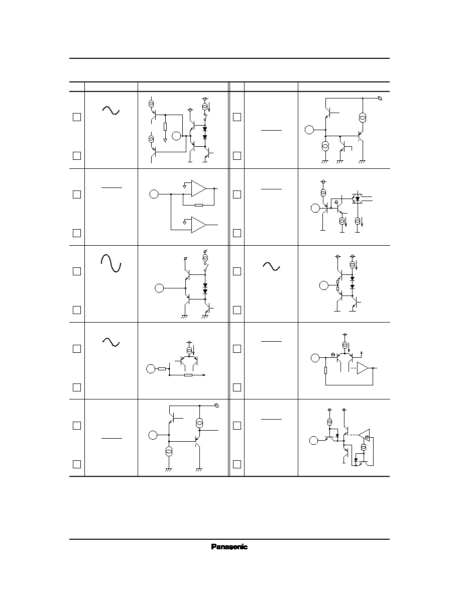
Pin No. Waveform ∑ Voltage
Equivalent circuit
Pin No. Waveform ∑ Voltage
Equivalent circuit
s
Pin Descriptions
(V
CC
or GND pins are not shown)
∑
DC 2.38V
DC 2.38V
DC 2.38V
LP EMPH
50
µ
A
20k
Rec
ON
+
≠
Rec
10k
3.5k
20
µ
A
8.5k
Ope. amp.
output
DC 1.65V
L.S IN
20
µ
A
100
µ
A
50
µ
A
DC 2.38V
LPF OUT
20
µ
A
50k
V
REF
DC 2.38V
CCA IN
DC 2.38V
CCA OUT
2.38 VDC,
Rec NR output
PB
1
(63)
3
(61)
4
(60)
5
(59)
6
(58)
13
(51)
12
(52)
10
(54)
8
(56)
7
(57)
+
≠
1
63
∑
1
60
3
61
∑
3
58
4
60
∑
4
57
5
59
∑
5
56
6
58
∑
6
55
7
57
7
54
8
56
∑
8
53
10
54
∑
10
51
11
52
∑
12
50
12
51
∑
13
49
Note) The indicated values are typical ones, and may depend on operating conditions or individual IC.
V
CC1
= 4.75V, and V
CC2
= 8.2V
A number without a square denotes a pin No. of the AN3986FBP, while a number with a square denotes a pin No. of the
AN3986FHP.
11
ICs for Video Camera
AN3986FBP, AN3986FHP
16
18
2.38 VDC,
Buffer OUT
DC 2.38V
DC 2.38V
∑
20
DC 2.38V
R/P SW
DC 2.38V
CCA IN
20k
VREF
50
µ
A
5.6k
10k
4.04k
11.91k
100k
50k
50k
≠
+
50k
50k
50
µ
A
2.5V
MUTE SW
14
(50)
19
20
22
23
25
(45)
(46)
(24)
(26)
(38)
(40)
(42)
15
(49)
17
18
16
13
50
14
48
∑
14
49
15
47
15
46
17
16
45
17
25
24
18
19
19
45
∑
43
∑
46
44
22
21
∑
24
23
∑
26
25
∑
38
36
∑
40
38
∑
42
40
23
22
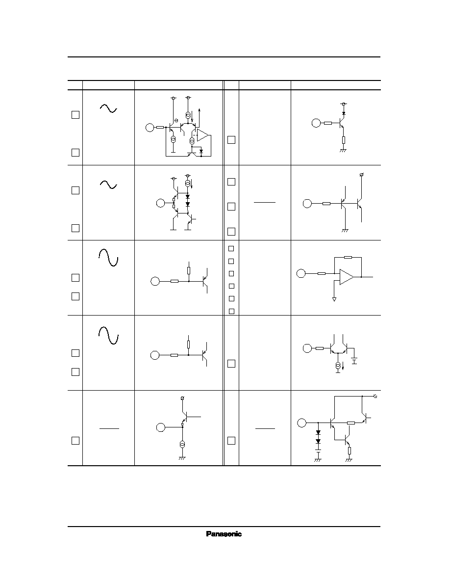
Pin No. Waveform ∑ Voltage
Equivalent circuit
Pin No. Waveform ∑ Voltage
Equivalent circuit
s
Pin Descriptions (cont.)
(V
CC
or GND pins are not shown)
Note) The indicated values are typical ones, and may depend on operating conditions or individual IC.
V
CC1
= 4.75V, and V
CC2
= 8.2V
A number without a square denotes a pin No. of the AN3986FBP, while a number with a square denotes a pin No. of the
AN3986FHP.
12
ICs for Video Camera
AN3986FBP, AN3986FHP
DC 2.38V
4.1V
V
REF
IN
DC
f=1.5MHz
(1.7MHz)
FM modulation
output
DC 2.3V
50
µ
A
10k
40k
20k
10
µ
A
Rec
ON
600
µ
A
10k
100k
HOLD
OFF
HOLD
OFF
DC 2.38V
RF IN
4VDC when not
active, and 0VDC
when active
27
(31)
65
(83)
66
68
69
(67)
(81)
(82)
28
39
(30)
(34)
(36)
41
(44)
64
(84)
70
(71)
∑
26
31
27
30
∑
62
83
65
79
∑
61
84
64
80
∑
67
71
70
68
∑
39
44
41
42
28
∑
27
30
∑
29
34
∑
32
36
34
66
∑
63
67
∑
64
81
∑
77
82
78
39
37
68
65
69
66
Pin No. Waveform ∑ Voltage
Equivalent circuit
Pin No. Waveform ∑ Voltage
Equivalent circuit
s
Pin Descriptions (cont.)
(V
CC
or GND pins are not shown)
Note) The indicated values are typical ones, and may depend on operating conditions or individual IC.
V
CC1
= 4.75V, and V
CC2
= 8.2V
A number without a square denotes a pin No. of the AN3986FBP, while a number with a square denotes a pin No. of the
AN3986FHP.
13
ICs for Video Camera
AN3986FBP, AN3986FHP
MM
60k
100k
100k
100k
25k
10k
20k
300k
f=30Hz,
square wave
73
76
78
72
79
73
70
76
72
78
74
72
69
79
75
Note) The indicated values are typical ones, and may depend on operating conditions or individual IC.
V
CC1
= 4.75V, and V
CC2
= 8.2V
A number without a square denotes a pin No. of the AN3986FBP, while a number with a square denotes a pin No. of the
AN3986FHP.
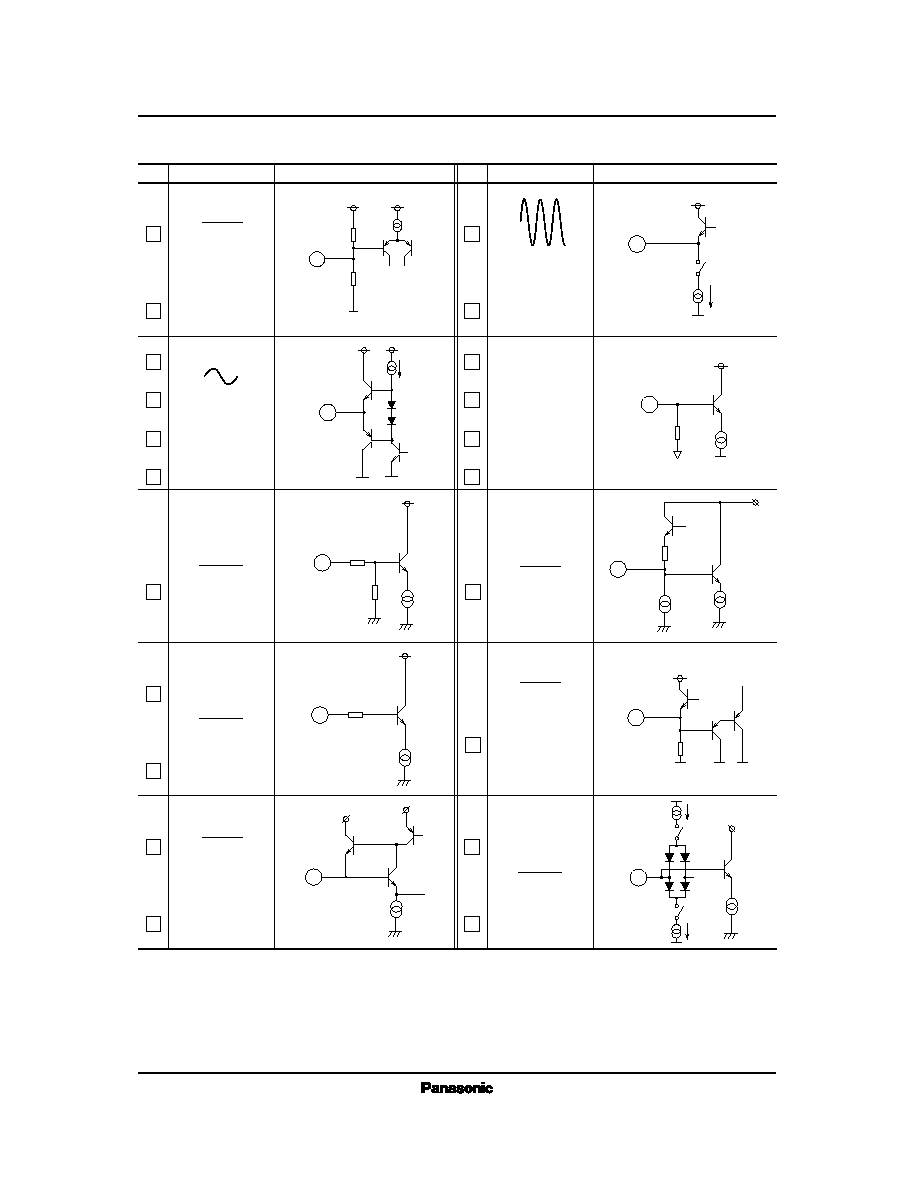
Pin No. Waveform ∑ Voltage
Equivalent circuit
Pin No. Waveform ∑ Voltage
Equivalent circuit
s
Pin Descriptions (cont.)
(V
CC
or GND pins are not shown)
s
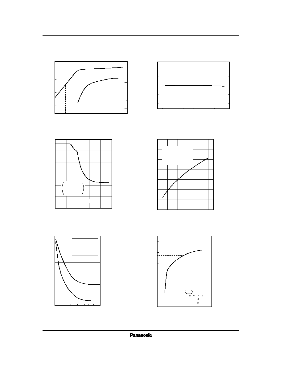
Reference
Power dissipation for the package
AN3986FHP P
D
--Ta
Ambient temperature Ta (∞C)
0
200
400
600
800
1,000
1,200
1,400
654
1,010
0
25
50
75
100
125
150
IC without heatsink
R
th≠a
=153∞C/W
P
D
= 654mW (25∞C)
On a glass-epoxy resin print board
(75
◊
75
◊
0.8t mm)
R
th≠a
= 99∞C/W
P
D
=1010mW (25∞C)
Power dissipation P
D
(mW)
NR decoder linearity characteristics
≠ 80
≠ 60
≠ 40
≠ 20
0
≠ 80
≠ 60
≠ 40
≠ 20
0
Line output level (dBs)
NR decoder input level (dBs)
V
CC1
= 4.75 (V)
V
CC2
= 8.20 (V)
f= 400Hz
20
20
14
ICs for Video Camera
AN3986FBP, AN3986FHP
s
Reference (cont.)
≠15
≠10
≠7
≠5
0
≠20
≠14
≠10
0
+10
0.01
0.02
0.05
0.1
0.2
Line AGC input/output characteristics
V
CC1
= 4.75 (V)
V
CC2
= 8.20 (V)
Level measurement at
f=400Hz
Distortion measurement at
f=1kHz
THD 5th with a 30kHz LPF
(Output level)
(Output distortion)
Line input level (dBs)
Line output level (dBs)
Line output distortion ratio (%)
Temperature characteristics of FM record output deviation
40
60
80
≠ 40
≠ 20
0
20
40
60
80
20
30
40
Temperature (∞C)
1.5 MHz side deviation (kHz)
1.7MHz side deviation (kHz)
V
CC1
= 4.75 (V)
V
CC2
= 8.20 (V)
V
in
= ≠ 20dBf
f= 400Hz
Line output level (dBs)
Fade control voltage (V)
≠100
≠ 80
≠ 60
≠ 40
≠ 20
0
1
2
3
4
4.75
0
Fade control output characteristics
V
CC1
= 4.75 (V)
V
CC2
= 8.20 (V)
Vin= ≠20dBs
f=1kHz
Using a 30 kHz LPF
0
2
4
6
8
10
12
4
5
6
7
8
9
Output subsystem supply voltage V
CC2
(V)
Line output maximum level (dBs)
Line maximum output level
V
CC1
= 4.75 (V)
THD 5th measured with a
1% distortion
f=1kHz
Using a 30kHz LPF
10k
load
14
1
10
30
100
≠70
≠ 60
≠50
Input carrier level (mV
P≠P
)
FM demodulator output noise (dBs)
1.5MHz side
1.7MHz side
V
CC1
= 4.75 (V)
V
CC2
= 8.20 (V)
≠16dBs reference
using a 30kHz LPF
50
20
2
3
5
Carrier level vs. FM
demodulator output noise
Headphone volume control output
HP volume control voltage (V)
HP output level (dBs)
8
39
Load
0
1
2
3
4
4.75
2.275
≠100
≠ 80
≠ 60
≠ 40
≠ 20
0
≠ 16dBs
≠ 26dBs
V
CC1
= 4.75 (V)
V
CC2
= 8.20 (V)
Vin= ≠ 20dBs
f= 400Hz
30kHz LPF