 | –≠–ª–µ–∫—Ç—Ä–æ–Ω–Ω—ã–π –∫–æ–º–ø–æ–Ω–µ–Ω—Ç: AN41204A | –°–∫–∞—á–∞—Ç—å:  PDF PDF  ZIP ZIP |
Product News
1 Kotari-yakemachi, Nagaokakyo, Kyoto 617-8520, Japan
Tel. +81-75-951-8151
http://panasonic.co.jp/semicon
Products and specifications are subject to change without notice.
Please ask for the latest Product Standards to guarantee the satisfaction
of your product requirements.
,
Overview
The AN41204A optical disc motor drive IC incorporates a
1-channel 3-phase full-wave PWM motor driver featuring
low vibration and noise as well as a 5-channel PWM output
driver for linear input. Integrating a spindle driver and
channel driver on a single chip and using small, thin
packaging reduces the mounting area. This helps to develop
equipment that is more compact, slim and lightweight.
Feature
∑ All-channel PWM driving power consumption is among the
lowest of its kind.
∑ Low-vibration and low-noise sinewave PWM is used to
drive the spindle section.
∑ Dead zone-less PWM driving for focus, tracking and tilt.
∑ Stepper motor drivers on two channels.
∑ Built-in thermal shutdown function.
∑ Compact, slim package.
Applications
Slim DVD recording units (RAM/+RW/-RW), optical disc units such as slim combination drives and car
navigation systems.
Achieving a 1-chip motor drive.
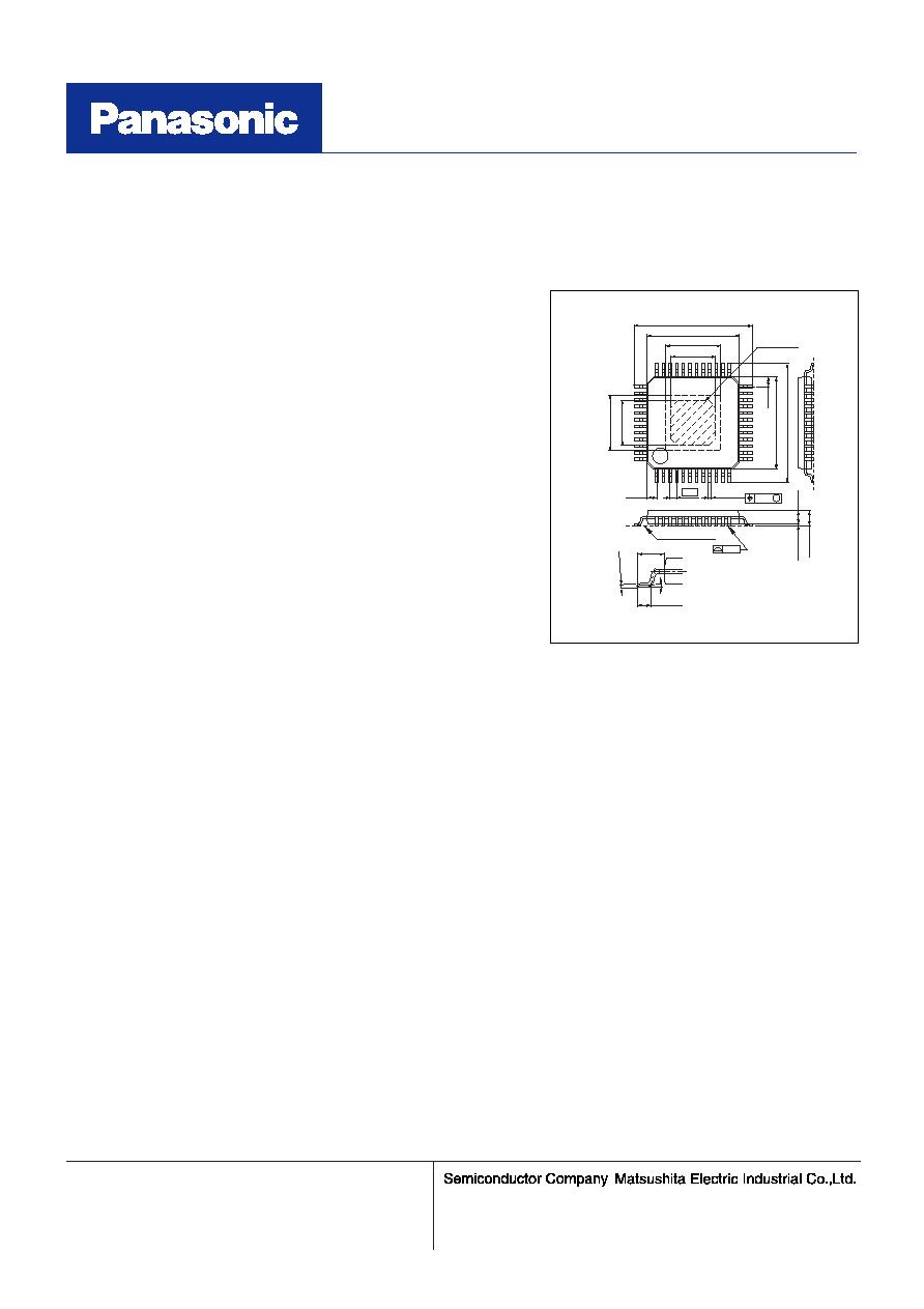
Optical Disc Motor Drive IC AN41204A
HQFP048-P-0707
New publication, effective from 19 Mar. 2004
M00631AE
Unit : mm
25
13
12
24
36
37
1
48
Area of no
resin flash
0.15
±
0.05
7.00
±
0.10
(0.75)
9.00
±
0.20
0∞ to 8∞
0.10
(1.00)
1.20 max
0.50
±
0.10
(1.00)
(4.20)
(3.37)
SEATING PLANE
0.50
(0.75)
0.20
±
0.05
9.00
±
0.20
7.00
±
0.10
(4.20)
(3.37)
≠0.05
+0.10
0.10
M
0.10
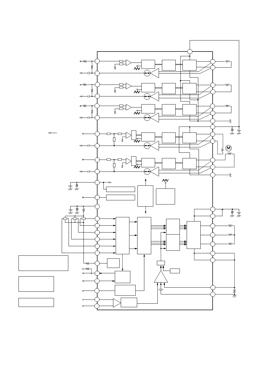
Block Diagram
STBY
V
REF
VREF reset (5-ch)
Logic
Pre-
drive
FB
Logic
Pre-
drive
FB
Logic
ABS
Pre-
drive
Triangular
wave
oscillator
Thermal
shut
down
(All)
FF
Hall
amp.
matrix
Hall
bias
Generate
FG
Upper
pre-
drive
Lower
pre-
drive
FB
OSC
3-phase
bridge
Rcs
Logic
Pre-
drive
FB
Logic
ABS
Pre-
drive
Power
MOS
FB
Power
MOS
Power
MOS
Power
MOS
Power
MOS
4
5
17
2
3
27
34
33
32
31
30
29
28
18
16
15
6
14
7
13
8
12
9
11
10
22
26
25
24
20
23
19
21
43
44
45
47
48
46
35
42
37
39
40
38
41
36
1
EC
ECR
SFG
BMS
FG
20k
100
VH
H3L
H3H
H2L
H2H
H1L
H1H
100
47
µ
F
5V
VDD
22
µ
F
1.65V
FB5
0.01µF
5
FB4
0.01µF
4
FB3
0.01µF
1.5k
15k 3
FB2
0.01µF
1.5k
15k 2
FB1
0.01µF
1.5k
15k 1
GND
CS
RCS2
RCS1
VMSP2
A2
A3
A1
VMSP1
47
µ
F
5V
Standby (all-ch)
PGST
RO5
FO5
RO4
FO4
VMST
PGAC
RO3
FO3
RO2
FO2
RO1
FO1
VMAC
47
µ
F
5V
H
OPEN
L
:1FG,All ch.=active
:3FG,All ch.=active
:1FG,ch.1 mute
H
OPEN
L
:R-BRK
:S-R-S-BRK
:S-BRK
EC<ECR
EC>ECR
:Acceleration
:BRK
3.3V
SFG Mode table
Spidle speed control signal input
FG
friequency select
FG
Signal output
Connect this part toV
REF
0.22
Distributor
Absolute
value
Brake mode
selector
BMS Mode table

Ch.1 non-inverted output
FO1
26
SP FG mode select input
SFG
2
Control circuit power supply
VDD
27
SP FG signal input
FG
3
SP Hall element 1 positive input
H1H
28
SP control signal input
EC
4
SP Hall element 1 negative input
H1L
29
SP reference voltage input
ECR
5
SP Hall element 2 positive input
H2H
30
Ch.5 control signal input
IN5
6
SP Hall element 2 negative input
H2L
31
Ch.4 control signal input
IN4
7
SP Hall element 3 positive input
H3H
32
Ch.3 control signal input
IN3
8
SP Hall element 3 negative input
H3L
33
Ch.2 control signal input
IN2
9
Hall-bias output
VH
34
Ch.1 control signal input
IN1
10
SP Motor drive power supply
VMSP1
35
Ch.1 feedback output
FB1
11
SP current detection
CS
36
Ch.2 feedback output
FB2
12
SP Driver output 1
A1
37
Ch.3 feedback output
FB3
13
SP Driver common Source output
RCS1
38
Ch.4 feedback output
FB4
14
SP Driver output 2
A2
39
Ch.5 feedback output
FB5
15
SP Driver output 3
A3
40
Ch reference voltage input
VREF
16
SP Driver common Source output
RCS2
41
SP Break mode select input
BMS
17
SP Motor drive power supply
VMSP2
42
Total shutdown input
STBY
18
Ch.4 and 5 Motor drive power supply
VMST
43
Ch.3 inverted output
RO3
19
Ch.4 non-inverted output
FO4
44
Ch.3 non-inverted output
FO3
20
Ch.4 inverted output
RO4
45
Ch.1 to 3 Coil drive GND
PGAC
21
Ch4 and 5 Motor drive GND
PGST
46
Ch1 to 3 Coil drive power supply
VMAC
22
Ch.5 non-inverted output
FO5
47
Ch.2 inverted output
RO2
23
CH5 inverted output
RO5
48
CH2 non-inverted output
FO2
24
GND
Symbol
Ch.1 inverted output
RO1
25
Control circuit GND
1
Description
Symbol
No
Description
No
Pin Descriptions
Absolute Maximum Ratings
Operating Supply Voltage Range
l=19,20,23,24,25,26,
44,45,47,48
V
7.0
V (l)
Drive output voltage
q=44,45,47,48
mA
±
1000
I (q)
Drive output current for
ch.4 and ch.5
Note) 4
o=37,38,39,40,41
mA
±
3000
I (o)
Drive power supply/output
instantaneous current
spindle
V
-0.3 to 6.0
VMSP,VMST,
VMAC,VDD
Supply voltage applied
range
2
mA
1200
IVMSP
Supply current
3000
IVMAC
2000
IVMST
3
mW
307.9
PD
Power dissipation
p=19,20,23,24,25,26
mA
±
1000
I (p)
Drive output current for
ch.1,2 and ch.3
m=37,39,40
V
7.0
V (m)
Drive output voltage
n=2,3,4,5,6,7,8,9,10,1
1,12,13,14,15,16,17,18
,28,29,30,31,32,33
V
GND to VDD
V (n)
Control signal input
voltage
100
IVDD
1
∞C
-55 to 150
Tstg
Storage temperature
x=34
mA
30
IHB(x)
Hall bias current
V
6.0
VMST,VMAC
VDD
Supply voltage
1
∞C
-30 to 85
Topr
Operating ambient
temperature
Note
Unit
Rating
Symbol
Parameter
Note)1: Ta = 25
∞C except storage temperature and operating ambient temperature.
2: Make sure that channels 1 to 5 do not have a current flow exceeding 1000 mA.
3: Power dissipation shows the value of only package at Ta = 85
∞C.
4: The above drive output current (
± 3000 mA) is permissible for a period exceeding 1 ms.
Note) Do not apply current or voltage from outside to any pin not listed above other than power supply and ground pin.
In the current circuit, (+) means current flowing into IC and (-) means current flowing out of IC.
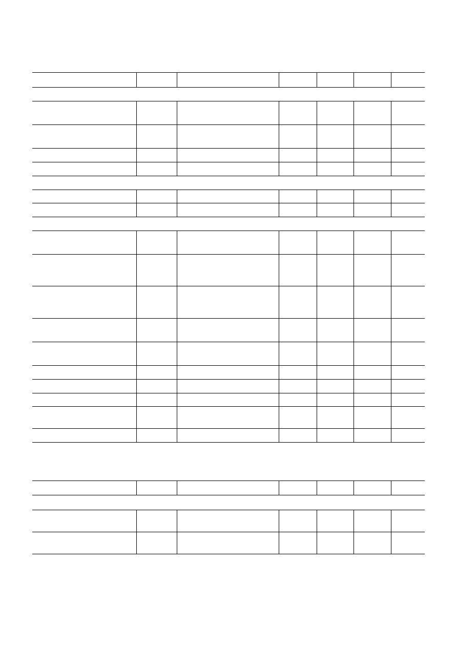
5.0
5.0
Typ.
V
5.5
3.5
VMAC
VMST
VMSP
V
5.5
4.0
VDD
Operating Supply Voltage Range
Unit
Max.
Min.
Symbol
Parameter

Electrical Characteristics
V
DD
=VMSP=VMAC=VMSL=5.0V,ECR=V
REF
=1.65V,STBY=3.3V,R
L
=8
Note) 1, Ta=25
∞C±2∞C unless otherwise specified.
0.50
0.32
I
O
=
-500mA
R
OH
Upper-side output-ON resistance
mA
1200
1000
800
R
CS
=0.22
I
TL
Torque limit current
<Hall amp.>
60
40
20
I
BH
=20mA
R
HB
Hall bias resistance
<Hall bias>
V
0.5
(Reset)
VRRL
Low-level input voltage
V
0.7
(Reset)
VSBL
STBY low-level input voltage
[Standby operation]
mV
88
50
7
INSP
DZ(+)
Dead zone (+)
V
2.2
1.1
INECR
Reference input voltage range
<Torque control>
<Output>
µA
1
-1
I
BH
Input bias current
A/V
1.59
1.33
1.07
R
CS
=0.22
A
CS
Input/Output gain
mV
88
50
7
INSP
DZ(
-)
Dead zone (+)
0.45
0.29
I
O
= 500mA
R
OH
Lower-side output-ON resistance
V
1.8
(Active)
VSBH
STBY high-level input voltage
µA
20
STBY=H
IDDS
Control supply current in
standby mode
mA
16
12
STBY=H
IDDA
Control supply current under no
input
[VREF Rest]
V
1.1
(Active)
VRRH
High-level input voltage
[SP Driver block]
µA
3
I
BH
Input bias current
V
4.0
2.5
1.5
V
HBR
Common-mode input voltage range
mVp-p
1000
200
50
V
INH
Allowable Input current
STBY=L
Condition
Typ.
µA
20
IVMS
Power supply current in
standby mode
Unit
Max.
Min.
Symbol
Parameter
(Reference values for design)
∞C
30
TTSD
Thermal shutdown
hysteresis width
[Thermal shutdown]
∞C
160
TTSD
Thermal shutdown circuit
operating temperature
Condition
Typ.
Unit
Max.
Min.
Symbol
Parameter
Electrical Characteristics
V
DD
=VMSP=VMAC=VMSL=5.0V,ECR=V
REF
=1.65V,STBY=3.3V,R
L
=8
Note) 1, Ta=25
∞C±2∞C unless otherwise specified.
<Brake mode selection switch>
<FG>
V
2.6
V
FG
=3.3V,I
FG
=
-0.01mA
R
FG
=20k
FGH
High-level FG output
V
0.2
V
FG
=3.3V,I
FG
=
-0.01mA
R
FG
=20k
FGL
Low-level FG output
V
2.6
VSFGH
High-level SFG input voltage
V
0.5
VSFGL
Low-level SFG input voltage
V
2.6
(Reverse Brake)
VBMGH
High-level BMS input voltage
V
0.5
(Short Brake)
VBMGL
Low-level BMS input voltage
mV
+50
-50
RL=8
VIN=VREF=1.65V
VOFS4
,5
Ch.4 and ch.5 output offset
voltage
mV
+70
-70
RL=8
VIN=VREF=1.65V
VOFS1
to 3
Ch.1 to ch.3 output offset
voltage
2.0
1.3
RL=8
RON2,
3
Ch.2 and ch.3 output-ON
resistance
(Upper + Lower)
[ch. Driver block]
kHz
288
230
172
FTR
PWM frequency
mV
40
25
10
RL=8
,RIN=0
VZD4,5
Ch4,5 input conversion
dead zone
2.3
1.5
RL=8
RON1
Ch.1 output-ON resistance
(Upper + Lower)
1.7
1.1
RL=8
RON4,
5
Ch.4 and ch.5 output-ON
resistance
(Upper + Lower)
dB
18.3
16.3
14.3
RL=8
,RIN=15k
G1,2,3
Ch.1 to ch.3 voltage gain(+)
dB
20.0
18.0
16.0
RL=8
,RIN=0
G4,5
Ch.4 and ch.5 voltage gain(+)
dB
+1.5
-1.5
RL=8
GR1to5
(+)/(
-) relative gain
Condition
Typ.
Unit
Max.
Min.
Symbol
Parameter
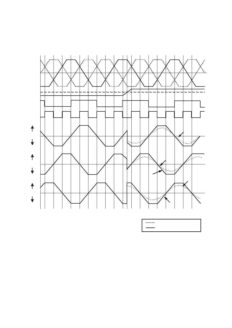
Phase Conditions of Hall Input and Output Current
H1
H2
H3
H1
H2
H3
BMS="L"
BMS="H"
BMS="H"
BMS="H"
BMS="L" or Open
IA3
IA1
IA2
FG1
FG3
ECR
EC
Hall
input
BMS="H" : Reverse Brake
BMS="L" : Short Brake
A
B
D
E
F
C
BMS="L"
Flow out
Flow in
Flow out
Flow in
Flow out
Flow in
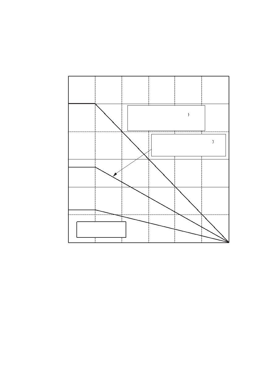
Package Dissipation
0
25
50
75
100
150
0
0.5
1.0
1.5
2.0
125
Independent IC
without a heat sink
Rth(j-a)=211.1 C/W
Rth(j-a)=92.7 C/W
2.510
2.5
3.0
1.348
0.592
Mounted on standard board (four layer)
(glass epoxy:50mm◊50mm◊0.8mm
Heatsink mounted
Rth(j-a)=49.8 C/W
Mounted on standard board (one surface )
(glass epoxy:50mm◊50mm◊0.8mm
With out heatsink mounted
Power dissipation
P
D
(W)
Ambient temperature
Ta ( C)