 | –≠–ª–µ–∫—Ç—Ä–æ–Ω–Ω—ã–π –∫–æ–º–ø–æ–Ω–µ–Ω—Ç: AN5276 | –°–∫–∞—á–∞—Ç—å:  PDF PDF  ZIP ZIP |
ICs for Audio Common Use
1
AN5276
5 W
◊
2-ch (19V, 8
) power amplifier with
variable audio output and volume control
s
Overview
The AN5276 is a monolithic integrated circuit designed
for 5.0 W (19 V, 8
) output audio power amplifier. It is
a dual channel SEPP IC suitable for stereo operation in
TV application.
s
Features
∑
Few external components :
∑ No Boucherot cells(output C, R)
∑ No Bootstrap Capacitors
∑ No Negative Feeback Capacitors
∑
Built-in muting circuit
∑
Built-in stand-by circuit
∑
Built-in various protection circuits
(Load-short, thermal, over-voltage and current)
∑
High ripple rejection(55 dB)
∑
Compatible with AN5275, AN5277
∑
Operating voltage range 10 V to 24 V(19 V typ.)
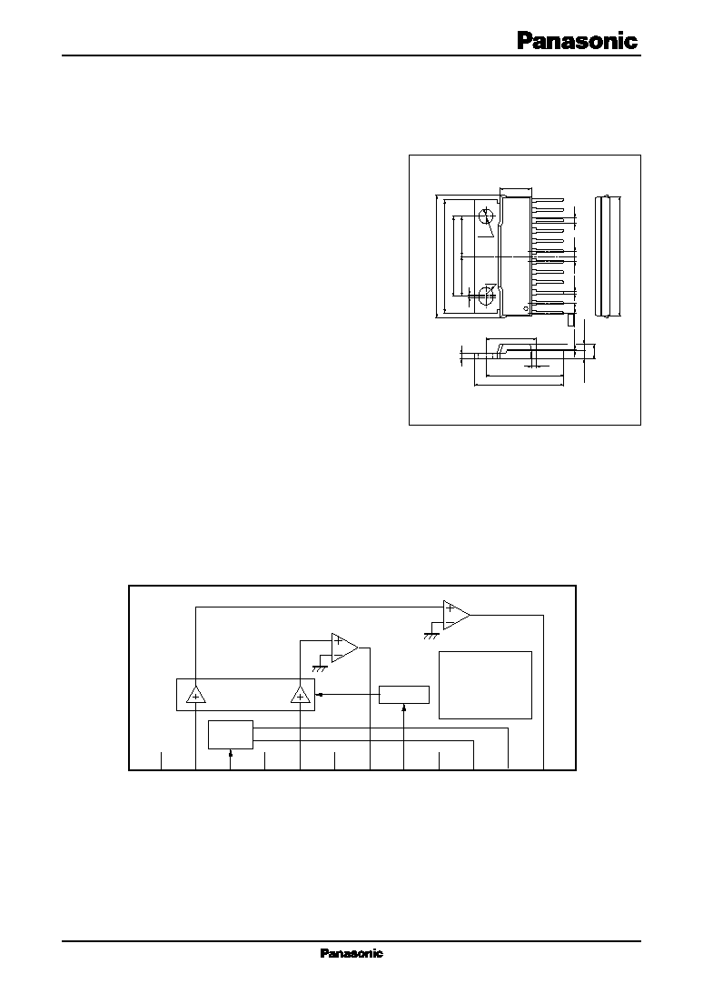
HSIP012-P-0000A
Unit : mm
7.7
±
0.3
(12.5)
19.1
±
0.3
21.9
±
0.3
(1.2)
(10.0)
(10.0)
29.6
±
0.3
20.0
±
0.3
0.6
28.0
±
0.3
29.75
±
0.30
3.6
R1.8
0.6
(1.27)
(1.27)
(1.3)
12
1
+0.15 ≠0.05
2.54
0.25
1.45
±
0.15
1.80
±
0.15
1.2
±
0.1
3.5
±
0.3
+0.10 ≠0.05
s
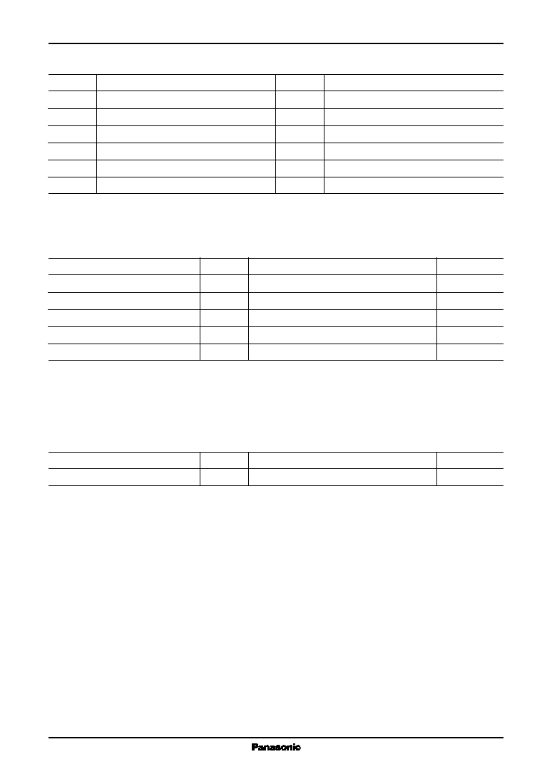
Block Diagram
N.C.
1
Ch.1 In
2
RF
3
GND
(Input)
4
Ch.2 In
5
N.C.
6
Out Ch.2
7
Mute
8
GND
(Output)
9
V
CC
10
Standby
11
Out Ch.1
12
Att. Con
Att.
Ripple
filter
Protection circuit
∑ Temperature
∑ Over-voltage
∑ Over-current
∑ Load short
s
Applications
∑
TV
2
AN5276
ICs for Audio Common Use
s
Absolute Maximum Ratings
Parameter
Symbol
Rating
Unit
Supply voltage
V
CC
26.0
V
Supply current
I
CC
4.0
A
Power dissipation
*2
P
D
37.5
W
Operating ambient temperature
*1
T
opr
-
25 to
+
75
∞
C
Storage temperature
*1
T
stg
-
55 to
+
150
∞
C
s
Recommended Operating Range
Parameter
Symbol
Range
Unit
Supply voltage
V
CC
10.0 to 24.0
V
Note) *1 : Except these items, all other measurements are taken at T
a
=
25
∞
C.
*2 : T
a
=
75
∞
C.
Pin No.
Descriptions
7
Ch.2 output
8
Mute
9
Output GND
10
V
CC
11
Standby
12
Ch.1 output
Pin No.
Descriptions
1
N.C.
2
Ch.1 input
3
Ripple filter
4
Input GND
5
Ch.2 input
6
N.C
s
Pin Descriptions
3
ICs for Audio Common Use
AN5276
s
Electrical Characteristics at V
CC
=
19 V, f
=
1 kHz, R
L
=
8
, T
a
=
25
∞
C
Parameter
Symbol
Conditions
Min
Typ
Max
Unit
Quiescent current
I
CQ
V
IN
=
0 mV
35
70
mA
Output end noise voltage
*1
V
NO
No input, R
g
=
10 k
0.22
0.4
mV
Voltage gain
G
V
V
IN
=
57 mV
32
34
36
dB
Total harmonic distortion
THD
V
IN
=
57 mV
0.2
0.4
%
Maximum Output Power
P
O
V
CC
=
22 V, THD
=
10 %
5.6
7.0
W
Maximum Output power
P
O
V
CC
=
19 V, THD
=
10 %
4.0
5.0
W
Ripple rejection ratio
*1
RR
V
r
=
1 V
rms
45
55
dB
f
r
=
120 Hz, R
g
=
10 k
Channel balance
CB
V
IN
=
57 mV
-
1.0
0
1.0
dB
Muting Ratio
MR
V
IN
=
57 mV
70
80
dB
Muting control voltage
V
MUTE
V
IN
=
57 mV, MR
70 dB
3.0
V
Standby control voltage 'on'
V
STD-ON
No input, I
CC
0.1 mA
5.0
V
Standby control voltage 'off'
V
STD-OFF
No input, I
CC
17 mA
8.5
V
Channel crosstalk
CT
V
IN
=
57 mV, R
g
=
10 k
50
60
dB
Note) *1 : For this measurement, use the 20 Hz to 20 kHz (12 dB/OCT) filter.

4
AN5276
ICs for Audio Common Use
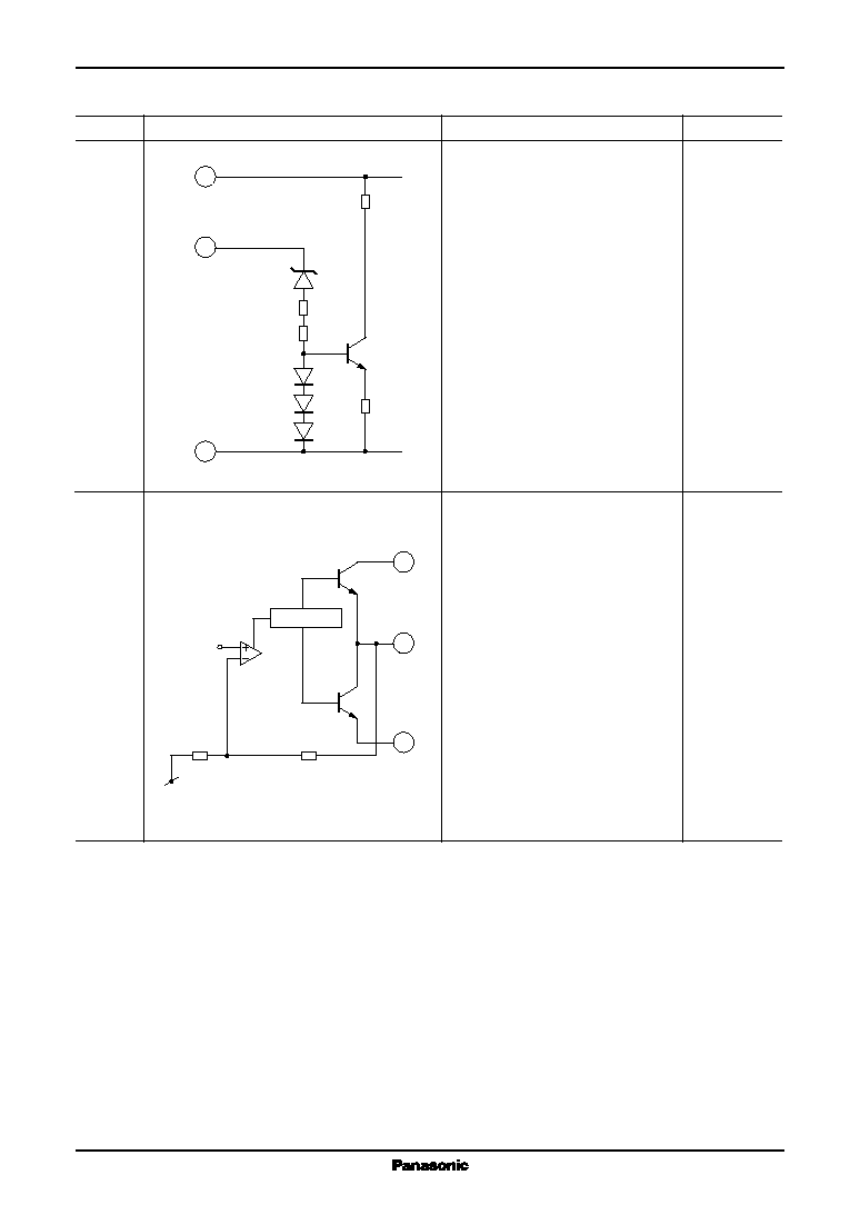
Pin No.
Equivalent circuit
Description
DC voltage (V)
1
Not connected
2
Ch.1 input
0
This is the amplifier input pin.
3
Ripple filter
V
CC
-1.5V
BE
This is the pin to connect the positive
terminal of a ripple filter capactior.
4
Input GND
0
Input ground pin
5
Ch.2 input
This is the amplifier input pin.
6
Not connected
s
Terminal Equivalent Circuits
2
4
200
400
30 k
10
3
4
30 k
20 k
15.7 k
15 k
5
4
200
400
30 k

5
ICs for Audio Common Use
AN5276
Pin No.
Equivalent circuit
Description
DC voltage (V)
7
Ch.2 output
V
CC
/2
Ch.2 output pin
8
Mute
Mute input pin.
Mute 'on'
=
5 V
Mute 'off'
=
0 V
9
Output GND
0
Ch.1 & Ch.2 output ground.
10
V
CC
19 V(typ.)
This is the power supply pin.
s
Terminal Equivalent Circuits (continued)
10
7
9
V
CC/2
30 k
600
Pre amp.
Driver Cct
10
8
4
3 k
3 k
10 k
200
6
AN5276
ICs for Audio Common Use
s
Terminal Equivalent Circuits (continued)
Pin No.
Equivalent circuit
Description
DC voltage (V)
11
Standby
This is the standby control pin.
12
Ch.1 output
V
CC
/2
Ch.1 output pin
10
11
4
5 k
5 k
3 k
10
12
9
30 k
600
Pre amp.
Driver Cct
7
ICs for Audio Common Use
AN5276
s
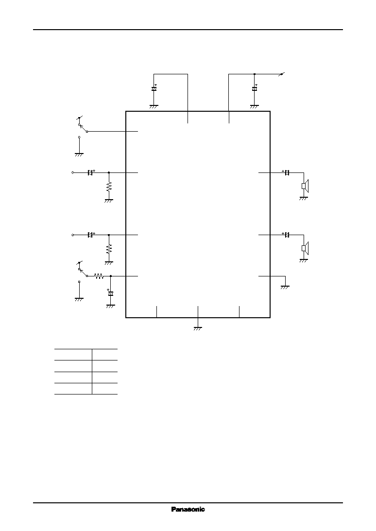
Application Circuit Example
s
Usage Notes
1) External heatsink is needed when used. External heatsink should be fixed to the chassis.
2) Fin of the IC can be connected to GND.
3) Please prevent output to V
CC
short and output to GND short.
4) The temperature protection circuit will operate at T
j
around 150
∞
C. However, if temperature decreass, the
protection circuit would automatically be deactivated and resume normal operation.
N.C.
1
Input GND
Output GND
4
6
N.C.
1
8
9
7
V
CC
V
CC
V
IN2
10 k
8.2 k
SP
8
10
µ
F
Mute
Mute on
Mute off
1000
µ
F
100
µ
F
1000
µ
F
12
SP
8
1000
µ
F
STB
R.F
.
STB off
5 V
STB on
8
5
1
µ
F
V
IN1
10 k
2
1
µ
F
11
STB off
V
CC
STB on
0 V
Mute off
0 V
Mute on
5 V
5 V
8
AN5276
ICs for Audio Common Use
s
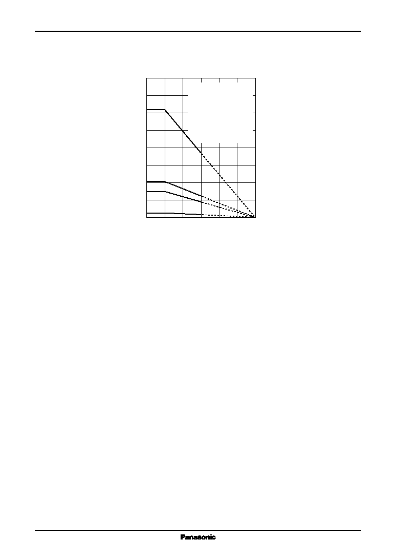
Technical Information
∑
P
D
T
a
curves of HSI P012-P-0000A
0
0
Po
wer dissipation P
D
(W)
Ambient Temperature T
a
(
∞
C)
25
50
75
100
125
150
10
20
30
40
50
60
70
80
20.8 W
62.5 W
(1)
(2)
(3)
(4)
15.6 W
3.0 W
(1) T
c
=
T
a
, 62.5
∞
C/W(
j-c
=
2
∞
C/W)
(2) 20.83 W(
f
=
4.0
∞
C/W)
With a 100cm
2
◊
3mm Al heat
sink (black colour coated) or a
200cm
2
◊
2mm Al heat sink (not
lacquered)
(3) 15.63 W(
f
=
6.0
∞
C/W)
With a 100cm
2
◊
2mm Al heat sink
(not lacquered)
(4) 3.0 W at T
a
=
25
∞
C(
j-a
= 4
2
∞
C/W)
Without heat sink
P
D
T
a