 | –≠–ª–µ–∫—Ç—Ä–æ–Ω–Ω—ã–π –∫–æ–º–ø–æ–Ω–µ–Ω—Ç: AN5491K | –°–∫–∞—á–∞—Ç—å:  PDF PDF  ZIP ZIP |
ICs for TV
1
AN5491K
Synchronous signal and deflection distortion correction processing IC
supporting I
2
C bus for HD, wide television
s
Overview
The AN5491K is a deflection processor IC for syn-
chronous signal processing and screen distortion correc-
tion. It synchronizes with the input signal of High-vision,
wide television, NTSC, PAL and VGA by the external
binary input signal of them so that a multimedia television
can be realized easily.
s
Features
∑
Supports the multiple-point horizontal frequency
(15.7 kHz to 62.7 kHz)
∑
Horizontal duty is controllable by external voltage.
∑
Built-in full functions for correction
(Horizontal and vertical: 16 items)
∑
Over-current detection, shut-down and hold-down
s
Applications
∑
High-vision televisions, Wide screen televisions and
Projection televisions
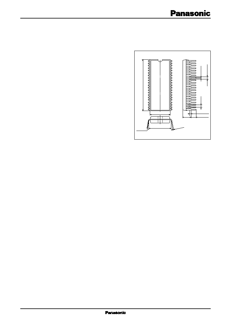
SDIP042-P-0600A
Unit: mm
0.5±0.1
0.9±0.25
1.778
13.7±0.3
15.3±0.25
3
∞
to 15
∞
0.96±0.25
4.76±0.25
3.3±0.25
1
2
3
4
5
6
7
8
9
10
11
12
13
14
15
16
17
18
19
20
21
42
41
40
39
38
37
36
35
34
33
32
31
30
29
28
27
26
25
24
23
22
0.3
+0.1
≠0.05
36.8±0.3
AN5491K
ICs for TV
2
s
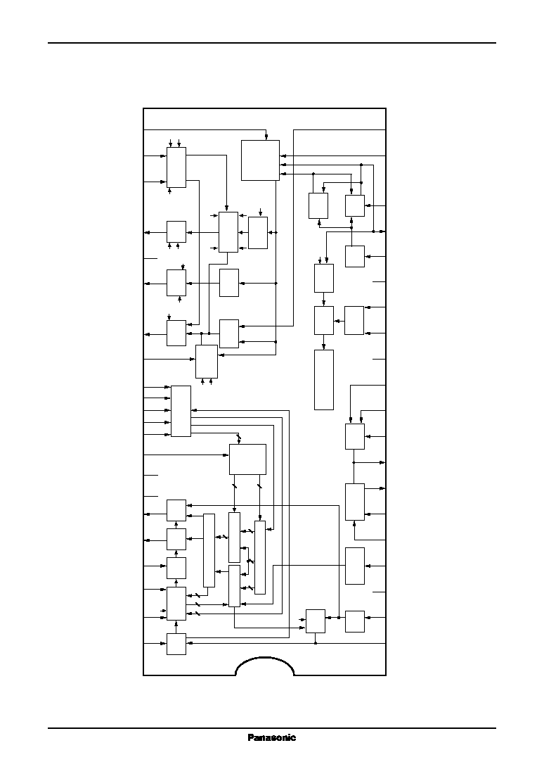
Block Diagram
42
H-AFC1
1
H-OSC
H-pulse in
FBP in
H-V
CC
H-AFC2
Shut down
H-duty adj.
Comparator ref.
H-out
Comparator in
Comparator out
BLK out
V-SAW upper
V-SAW lower
V-SAW in
I
2
L V
CC
SDA
SCL
DEF V
CC
VP in
VS2
V-OSC
Ramp
Trapezoid
Lock det.
H-GND
I
2
L GND
VGA
◊
1
◊
2
◊
4
◊
8
◊
32
Corner level
EW out
Phase out
DEF GND
V-out
41
2
40
3
39
4
38
5
37
6
36
7
34
8
27
9
35
31
26
10
19
25
11
33
12
32
13
14
30
15
29
16
28
17
18
24
23
20
22
21
EHT-DC
EHT-AC
AGC
H
VCO
H
AFC2
H-POS
Gain-SW
Counter BF
H
duty
H
out
V
out
V
OSC
V-
A
G
C
timing
V
-latch
pulse
Data
latch
Sync. DEF D
A
C
I
2
C
decode
VP
slice
HP
slice
H
AFC1
V
-
BLK
gen.
Shut do
wn
det.
X-ray
det.
V/I
con
v
erter
Phase
out
V-
S
A
W
correction
EHT
correction
Ramp
/A
GC
Lock
det.
EW
out
T
rapezoid
crrection
Upper
Latch-SW
H-parabola
V-
L
I
N
BO
W
V-
S
Lo
wer
V
-amp.
Phase
crrection
Counter
input
Corner
correction
f
H
switch
input
Counter
Counter PG
Counter decode
2
2
2
4
7
2
6
5
2
7
V
-
POS
POL
P
arallel
V
-
EHT
H- EHT
T
rape
H-WID
EHT
-A
C
ICs for TV
AN5491K
3
s
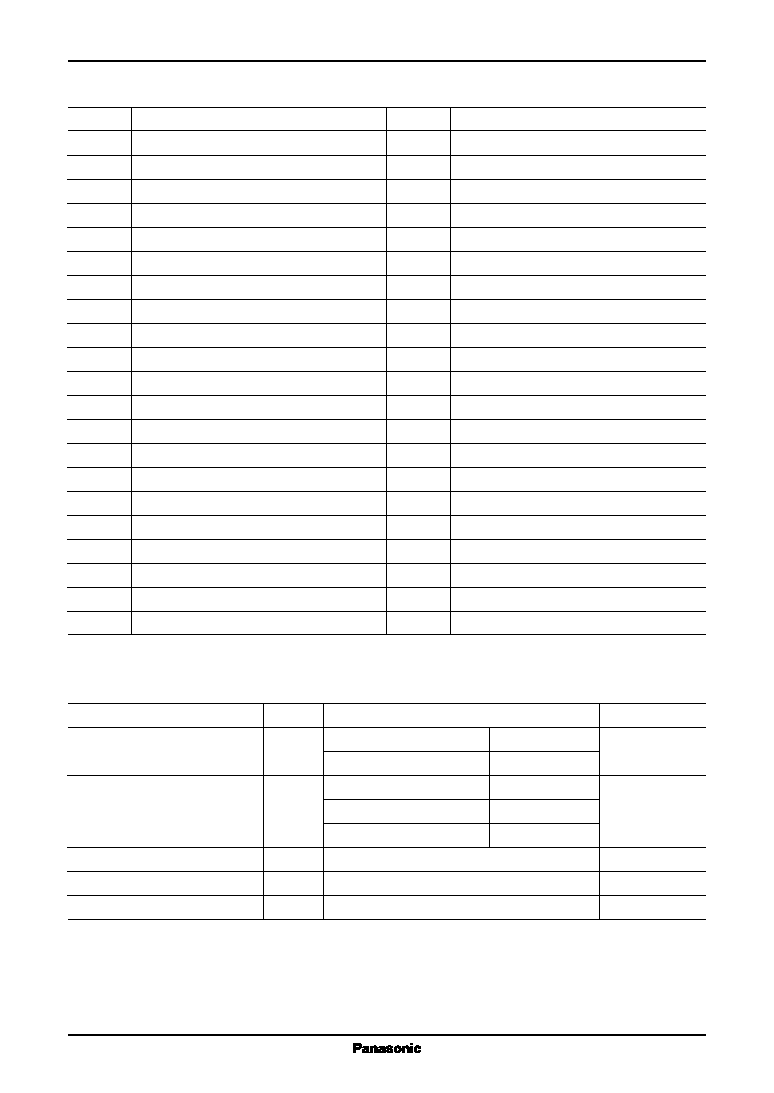
Pin Descriptions
s
Absolute Maximum Ratings
Pin No.
Description
Pin No.
Description
1
H-AFC1
22
V-AGC
2
H-pulse input
23
EHT-DC input
3
H-V
CC
(6.2 V)
24
EHT-AC input
4
Shut down SW
25
◊
8
5
Comparator ref. (6.5 V)
26
◊
4
6
Comparator
27
VGA
7
Comparator output
28
V-output
8
BLK output
29
DEF GND
9
V-SAW slice voltage (High)
30
Phase output
10
V-SAW slice voltage (Low)
31
◊
2
11
V-SAW input
32
EW output
12
I
2
L V
CC
(5 V)
33
Corner slice voltage
13
I
2
C SDA input
34
I
2
L GND
14
I
2
C SCL input
35
◊
1
15
DEF V
CC
(9 V)
36
H-GND
16
V-pulse input
37
Lock det.
17
V-pulse output
38
H-output
18
V-OSC
39
H-duty
19
◊
32
40
H-AFC2
20
V-ramp
41
FBP input
21
Trapezoid correction voltage
42
H-OSC
Note) *1: Except for the operating ambient temperature and storage temperature, all ratings are for T
a
=
25
∞
C.
*2: The power dissipation shown is for the independent IC without a heat sink in free air at T
a
=
70
∞
C.
Parameter
Symbol
Rating
Unit
Supply voltage
V
CC
V
CC1
5.6
V
V
CC2
10
Supply current
I
CC
I
CC1
24
mA
I
CC2
29
I
3
14
Power dissipation
*2
P
D
600
mW
Operating ambient temperature
*1
T
opr
-
20 to
+
70
∞
C
Storage temperature
*1
T
stg
-
55 to
+
150
∞
C

AN5491K
ICs for TV
4
s
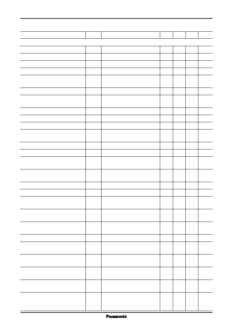
Recommended Operating Range
Parameter
Symbol
Range
Unit
Supply voltage
V
CC1
4.5 to 5.0 to 5.5
V
V
CC2
8.1 to 9.0 to 9.9
s
Electrical Characteristics at T
a
=
25
∞
C
Parameter
Symbol
Conditions
Min
Typ
Max
Unit
DC characteristics
Circuit current I
CC1
I
12
V
CC1
=
5 V, V
CC2
=
9 V
13.6
17.0
20.4
mA
Circuit current I
CC2
I
15
V
CC1
=
5 V, V
CC2
=
9 V
16.8
21.0
25.2
mA
Circuit current I
CC3
I
3
V
CC1
=
5 V, V
CC2
=
9 V,
6.0
7.5
9.0
mA
V
CC3
=
6.5 V
Synchronizing signal processing
Horizontal free-running oscillation
f
HO8
Pin 2: Without input, Pin 25: High
61.5
62.7
63.9
kHz
frequency 1 [Divide-by-8]
Pins 19, 26, 31, 35: Low
Horizontal free-running oscillation
f
HO16
Pin 2: Without input
30.8
31.4
32.0
kHz
frequency 2 [Divide-by-16]
Pins 19, 25, 26, 31, 35: Low
Horizontal free-running oscillation
f
HO32
Pin 2: Without input
15.4
15.7
16.0
kHz
frequency 3 [Divide-by-32]
Pin 19: High
Horizontal output pulse duty cycle 1
HO1
Pin 2: Without input, Pin 39: 2 V
11.7
14.0
16.6
µ
s
[Divide-by-32]
Pin 19: High
Horizontal output pulse duty cycle 2
HO2
Pin 2: Without input, Pin 39: 5 V
23.9
28.5
33.7
µ
s
[Divide-by-32]
Pin 19: High
Horizontal high-level output voltage
V
FHH
DC voltage for pin 38 high-level
2.8
3.5
4.2
V
Horizontal low-level output voltage
V
FHL
DC voltage for pin 38 low-level
0
0.3
V
Horizontal output start voltage
V
FHS
Minimum voltage of pin 3 to bec-
4.2
5.0
V
ome f > 10 kHz when horizontal
oscillation output is 1 V[p-p] or
more in divide-by-32 mode.
Screen center variable range 1
t
DH16
Pin 25: Low,
2.16
2.70
3.24
µ
s
[Divide-by-16]
Pins 19, 26, 31, 35: High
Change amount of phase difference
between H
P
and H-out of Data 08:
[00] to [1F]
Screen center variable range 2
t
DH32
Pin 19: Low,
3.8
4.8
5.8
µ
s
[Divide-by-32]
Change amount of phase difference
between H
P
and H out of Data 08:
[00] to [1F]
Horizontal input pulse threshold voltage
V
T2
Slice level of pin 2
0.9
1.5
2.1
V
Over-voltage protective operation
V
4
Pin 4 voltage at I
4
=
50
µ
A
0.60
0.75
0.90
V
voltage
ICs for TV
AN5491K
5
s
Electrical Characteristics at T
a
=
25
∞
C (continued)
Parameter
Symbol
Conditions
Min
Typ
Max
Unit
Deflection correction processing
V
P
pulse for OSD low-level
V
LOSD
V
CC1
=
5 V, V
CC2
=
9 V
0
0.4
V
V
P
pulse for OSD high-level
V
HOSD
V
CC1
=
5 V, V
CC2
=
9 V
2.2
2.75
3.3
V
EHT-AC input pin voltage
V
24
Pin 24: Open
2.00
2.45
2.90
V
Vertical input signal threshold voltage
V
TFV
Pin 16: Input
0.9
1.5
2.1
V
Vertical free-running oscillation
f
VO
Pin 16: Without input
35
44
53
Hz
frequency
external R
=
10 k
, C
=
3.3
µ
F
Typical vertical output amplitude
V
V
V amplitude DAC: Typ.
0.88
1.10
1.32
V[p-p]
Typical EW output amplitude
V
EW
EW output amplitude for typical ver-
0.8
1.0
1.2
V[p-p]
tical output amplitude
=
1.25 V[p-p]
Phase out amplitude
V
PHASE
Side pin parallel, DAC: Typ.
-
0.1
0
0.1
V[p-p]
Ramp waveform amplitude
V
RAMP
f
V
=
50 Hz to 120 Hz
2.15
2.45
2.75
V[p-p]
AGC input and output current
I
AGC
1.6
2.0
2.4
mA
Service SW: ON time
V
28SW
3.1
3.5
3.9
V
Vertical output DC
BLK pulse high-level
V
HBLK
4.5
5.0
5.5
V
BLK pulse low-level
V
LBLK
0
0.4
V
Vertical output amplitude
V
AMPmax
V amplitude ratio between
+
40
+
50
+
60
%
variable ratio (max.)
typ.
max.
Vertical output amplitude
V
AMPmin
V amplitude ratio between
-
40
-
50
-
60
%
variable ratio (min.)
typ.
max.
Vertical output DC variable amount (min.)
V
SHIFTmin
Vertical DC: Typ.
min.
-
0.28
-
0.38
-
0.48
V
Vertical output DC variable amount (max.)
V
SHIFTmax
Vertical DC: Typ.
max.
+
0.28
+
0.38
+
0.48
V
Vertical output trapezoidal waveform
V
TRAPmin
Trapezoidal waveform correction:
-
0.28
-
0.38
-
0.48
V
correction variable amount (min.)
Typ.
min.
Vertical output trapezoidal waveform
V
TRAPmin
Trapezoidal waveform correction:
+
0.28
+
0.38
+
0.48
V
correction variable amount (max.)
Typ.
max.
External trapezoidal waveform
V
21
2.4
3.0
3.6
V
center voltage
Vertical output center DC level
V
28
2.8
3.5
4.2
V
EW output (min.) to parabolic
V
EWmin
Parabolic amplitude: Min.
-
0.1
0
0.1
V[p-p]
amplitude change
EW output (max.) to parabolic
V
EWmax
Parabolic amplitude: Max.
1.4
1.8
2.2
V[p-p]
amplitude change
EW output (min.) (DC)
V
EWmin
Horizontal amplitude: Min.
-
0.95
-
1.15
-
1.35
V
to horizontal amplitude change
EW output (max.) (DC)
V
EWmax
Horizontal amplitude: Max.
+
0.95
+
1.15
+
1.35
V
to horizontal amplitude change
EW output (bottom voltage) 1
V
EDC1
EHT-DC: 5.0 V
3.8 V
+
1.04
+
1.30
+
1.56
V
to EHT-DC change
Horizontal EHT: Max.
EHT-AC gain: Min.