 | –≠–ª–µ–∫—Ç—Ä–æ–Ω–Ω—ã–π –∫–æ–º–ø–æ–Ω–µ–Ω—Ç: AN5764N | –°–∫–∞—á–∞—Ç—å:  PDF PDF  ZIP ZIP |

ICs for TV
1
AN5764N
Horizontal picture position control IC for CRT monitor
s
Overview
The AN5764N is an IC for CRT monitor horizontal
picture position control. The picture position can be con-
trolled by DC voltage, and the adoption of fin-attached
SIL 7-pin package contributes to the rationalization of
monitor set.
s
Features
∑
CRT monitor position control
∑
Built-in low voltage output circuit
∑
Built-in DC control circuit
s
Applications
∑
CRT monitor
s
Block Diagram
HSIP007-P-0000
Unit: mm
GND
Control circuit
4
V
CC
1
N.C.
7
2
6
3
5
V-REG
(7.80)
(6.40)
7
R1.80
0.60
(4.20)
1
(1.20)
(1.00)
(0.30)
(0.83)
2.54
0.60
±0.10
1.45
±0.20
1.80
±0.20
3.50
±0.30
0.35
+0.10
≠0.05
(3.80) (3.80)
15.30
±0.20
(17.10)
1.20
±0.10
7.70
±0.20
22.00
±0.30
16.90
±0.30
3.60
±0.10
12.50
±0.10
2.80
±0.10
s
Pin Descriptions
Pin No.
Description
1
V
CC
2
Constant voltage output (3 V)
3
Control input
4
GND
5
Out1 (Positive output)
6
N.C.
7
Out2 (Negative output)
Note) The fin is at the same potential as GND.
AN5764N
ICs for TV
2
s
Absolute Maximum Ratings
Parameter
Symbol
Rating
Unit
Supply voltage
V
CC
8.0
V
Supply current
I
CC
500
mA
Power dissipation
*2
P
D
1 400
mW
Operating ambient temperature
*1
T
opr
-
20 to
+
75
∞
C
Storage temperature
*1
T
stg
-
55 to
+
150
∞
C
Note) *1: Except for the operating ambient temperature and storage temperature, all ratings are for T
a
=
25
∞
C.
*2: The power dissipation shown is for the independent IC without a heat sink at T
a
=
75
∞
C. (Refer to "s Application Note".)
s
Recommended Operating Range
Parameter
Symbol
Range
Unit
Supply voltage
V
CC1 , 2
5 to 7
V
Control input
V
3
-
4
0 to V
2
V
Out1 output maximum output current
I
5max
-
400 to
+
400
mA
Out2 output maximum output current
I
7max
-
400 to
+
400
mA
Constant voltage maximum output current
I
2max
-
2.0 to
+
0.02
mA
Note) For the circuit currents, '
+
' denotes current flowing into the IC, and '
-
' denotes current flowing out of the IC.
Parameter
Symbol
Conditions
Min
Typ
Max
Unit
Circuit current pin 1
I
CC1
V
CC
=
5.5 V, V
3
=
1.5 V
7
14
28
mA
At load (R
L
)
=
Open
Circuit voltage pin 2
V
2
-
4
V
CC
=
5.5 V, V
3
=
1.5 V
2.8
3.0
3.2
mA
At load (R
L
)
=
Open
Circuit voltage pin 5
V
5
-
4
V
CC
=
5.5 V, V
3
=
1.5 V
2.3
2.6
2.9
V
At load (R
L
)
=
Open
Circuit voltage pin 7
V
7
-
4
V
CC
=
5.5 V, V
3
=
1.5 V
2.3
2.6
2.9
V
At load (R
L
)
=
Open
Circuit voltage pin 5
-
7
V
5
-
7
V
CC
=
5.5 V, V
3
=
1.5 V
-
0.35
0.0
0.35
V
At load (R
L
)
=
Open
Out1 high-level output voltage
V
5HI
V
CC
=
5.5 V, V
3
=
3 V
4.2
4.5
4.7
V
At R
L
=
7.5
connection
Out1 low-level output voltage
V
5LOW
V
CC
=
5.5 V, V
3
=
0 V
1.3
1.8
2.3
V
At R
L
=
7.5
connection
Out2 high-level output voltage
V
7HI
V
CC
=
5.5 V, V
3
=
0 V
4.3
4.5
4.7
V
At R
L
=
7.5
connection
Out2 low-level output voltage
V
7LOW
V
CC
=
5.5 V, V
3
=
3 V
1.3
1.8
2.3
V
At R
L
=
7.5
connection
Output voltage difference min.
V
5
-
7min
V
CC
=
5.5 V, V
3
=
0 V
-
3.2
-
2.5
-
2.2
V
At R
L
=
7.5
connection
s
Electrical Characteristics at T
a
=
25
∞
C
ICs for TV
AN5764N
3
Parameter
Symbol
Conditions
Min
Typ
Max
Unit
Output voltage difference typ.
V
5
-
7typ
V
CC
=
5.5 V, V
3
=
1.5 V
-
0.4
0.0
0.4
V
At R
L
=
7.5
connection
Output voltage difference max.
V
5
-
7max
V
CC
=
5.5 V, V
3
=
3 V
2.2
2.5
3.2
V
At R
L
=
7.5
connection
s
Electrical Characteristics at T
a
=
25
∞
C (continued)
∑
Design reference data
Note) The characteristics listed below are theoretical values based on the IC design and are not guaranteed.
Parameter
Symbol
Conditions
Min
Typ
Max
Unit
Control input pin circuit current
I
3min
Current of pin 3,
-
100
-
10
0
µ
A
max.
at V
CC
=
5.5 V, V
4
=
0 V
Control input pin circuit current
I
3max
Current of pin 3,
-
50
-
5
0
µ
A
typ.
at V
4
=
0.5 V to 3 V
Out1 maximum output current
I
5max
Output current of pin 5,
300
400
mA
(Positive)
at V
CC
=
5.5 V
Out1 maximum output current
I
5min
Output current of pin 5,
-
400
-
300
mA
(Negative)
at V
CC
=
5.5 V
Out2 maximum output current
I
7max
Output current of pin 7,
300
400
mA
(Positive)
at V
CC
=
5.5 V
Out2 maximum output current
I
7min
Output current of pin 7,
-
400
-
300
mA
(Negative)
at V
CC
=
5.5 V
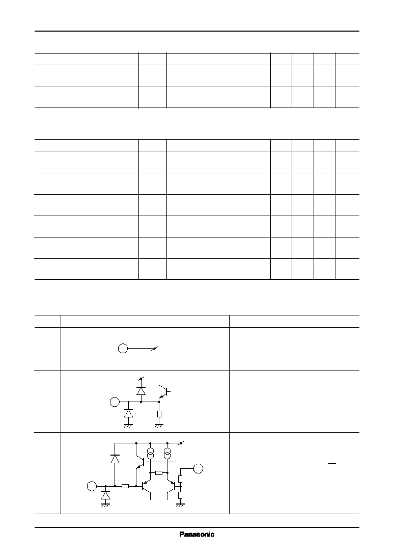
Pin No.
Equivalent circuit
Description
1
V
CC
:
Power supply pin
DC 5.5 V (typ.) application
2
Constant voltage output:
3 V constant-voltage output
DC 3 V
3
Control input:
Input pin for control
Output voltage balances at (V
3
=
1
V
2
)
2
0 V to 3 V variable
s
Terminal Equivalent Circuits
1
V
CC
2
30 k
V
CC
3
2
V
CC
15 k
30 k
3 V
0.9 V
30 k
AN5764N
ICs for TV
4
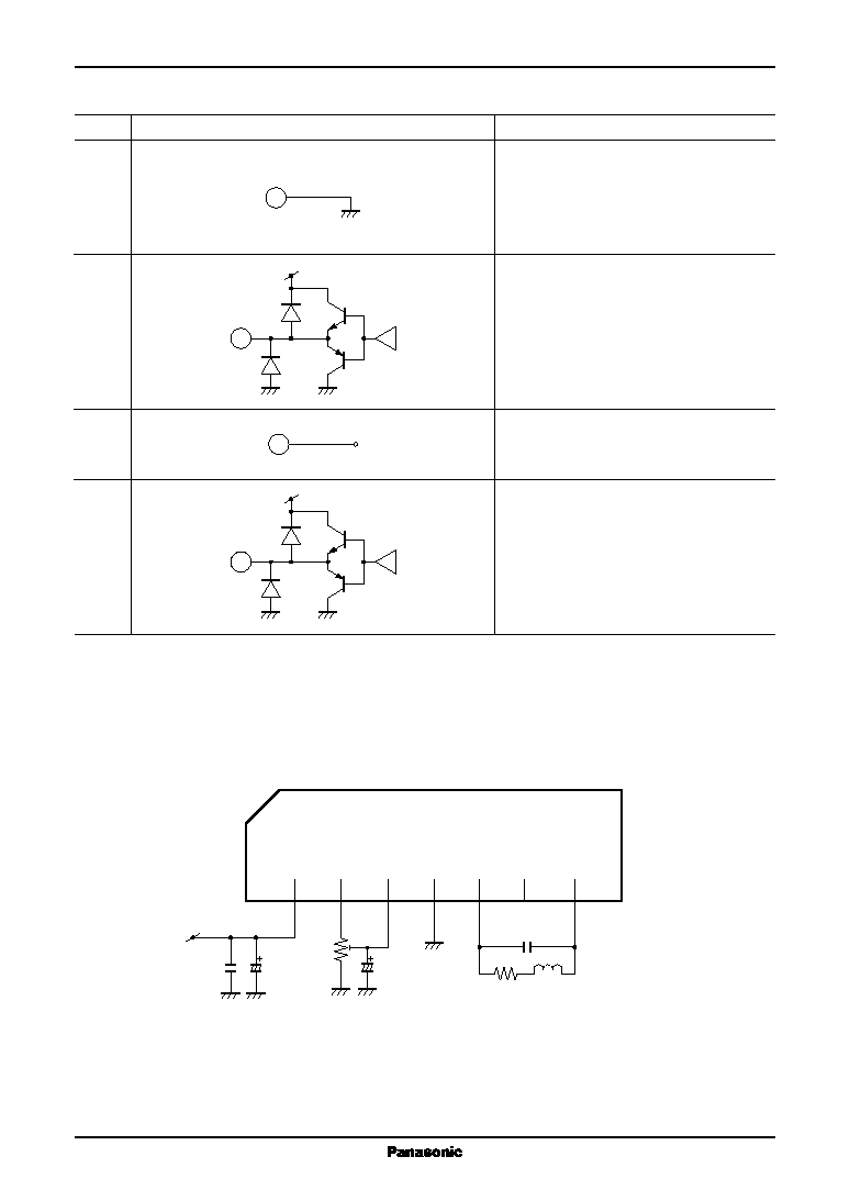
Pin No.
Equivalent circuit
Description
4
GND:
GND (Earth) pin
Fin becomes the same potential, too.
0 V
5
Out1 output:
Output pin
Outputs the same polarity as pin 3 control
voltage
DC 1.2 V to 4.3 V
6
N.C.:
N.C. pin
7
Out2 output:
Output pin
Outputs the reverse polarity of pin 3 control
voltage.
DC 1.2 V to 4.3 V
s
Terminal Equivalent Circuits (continued)
4
5
V
CC
6
7
V
CC
s
Application Circuit Examples
1
V
CC
2
3
4
GND
5
6
7
10
µ
F
8 V
1
µ
F
0.22
µ
F
0.1
µ
F
5 kB
7.5
ICs for TV
AN5764N
5
s
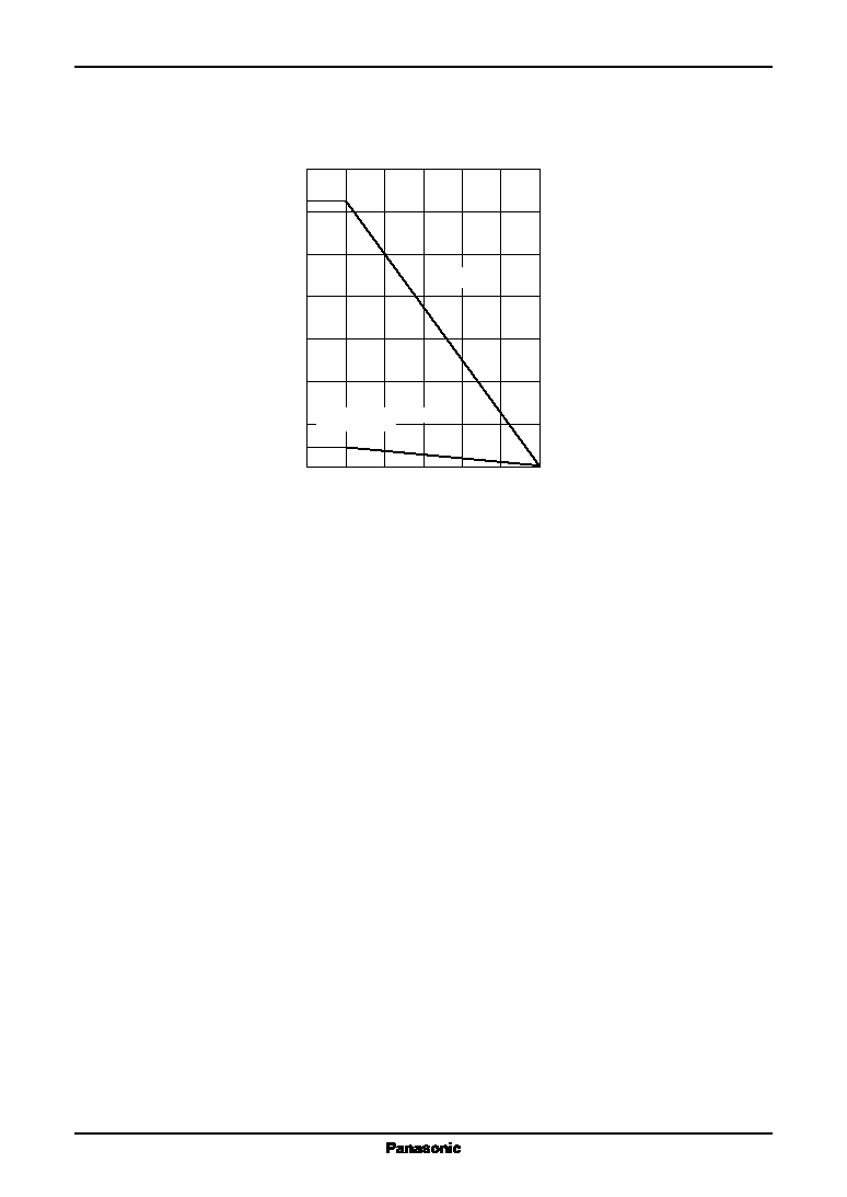
Application Note
∑
P
D
T
a
curve of HSIP007-P-0000
P
D
T
a
Po
wer dissipation P
D
(W)
0.000
0
25
150
Ambient temperature T
a
(
∞
C)
50
75
100
125
5.000
10.000
15.000
20.000
25.000
30.000
2.350
35.000
31.250
Infinite heat sink
R
th(j
-
c)
=
4.0
∞
C/W
Independent IC without a heat sink
R
th(j
-
a)
=
53.2
∞
C/W