 | ÐлекÑÑоннÑй компоненÑ: AN6095SH | СкаÑаÑÑ:  PDF PDF  ZIP ZIP |
Äîêóìåíòàöèÿ è îïèñàíèÿ www.docs.chipfind.ru
ICs for Mobile Communication
1
Publication date: December 2001
SDM00003BEB
AN6095SH
Reception IF
+ transmission quadrature modulation IC for PHS and
cellular telephone
I Overview
The AN6095SH is a single chip IC for PHS reception
IF block and transmission block.
Reception IF block is incorporating a 2nd down-mixer
and a limiter/RSSI circuit which can operate for up to
300 MHz of input frequency. Transmission block is in-
corporating a quadrature modulator, a phase shifter, an
up-mixer for 1.9 GHz and output level control functions.
It contributes to realization of small package and small
size of equipment.
I Features
· Operating supply voltage range: 2.7 V to 4.0 V
· Current consumption
Transmission block: 28 mA
Reception block: 5.3 mA
Sleep mode: 10
µA or less
(Transmission block)
· Output level: -8 dBm
· Output frequency: up to 2 GHz
· Transmission IF frequency: 100 MHz to 300 MHz
(Reception block)
· RSSI input D range: 80 dB
· Mixer conversion gain: 16 dB
· Limiter voltage gain: 70 dB
· 2nd down-mixer NF: 6 dB
I Applications
· PHS
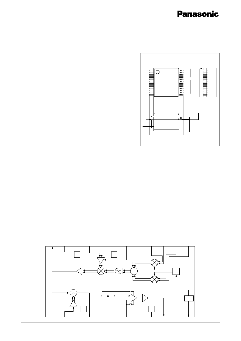
SSOP024-P-0300A
Unit: mm
5.5±0.3
7.5±0.3
(0.5)
0.1±0.1
0.15
+0.1 -
0.05
0.65±0.1
1.5±0.2
0.65±0.1
6.5±0.3
0.5
0.2±0.1
1
12
24
13
I Block Diagram
24
23
22
21
20
19
18
17
16
15
14
13
1
2
3
4
5
6
7
8
9
10
11
12
I
o
I
o
I
o
I
o
RSSI
Note) The package of this product will be changed
to lead-free type (SSOP024-P-0300D). See the
new package dimensions section later of this
datasheet.

AN6095SH
2
SDM00003BEB
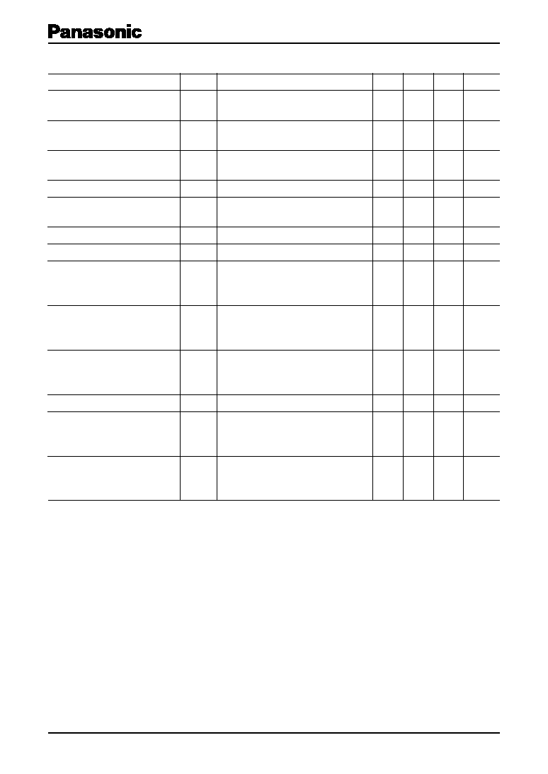
I Pin Descriptions
Pin No.
Symbol
Description
1
RXMXIN
RX-mixer-in
2
RXLOIN
RX-local-in
3
VCCM
V
CC
-mixer
4
MXO
Mixer-out
5
LMDEC1
Limiter-decouple 1
6
LMIN
Limiter-in
7
LMDEC2
Limiter-decouple 2
8
GNDR
GND-RX
9
VCCL
V
CC
-limiter
10
LMO
Limiter-out
11
TXLO1
TX-local 1-in
12
RSO
RSSI-out
Pin No.
Symbol
Description
13
Q-IN
Q-input
14
Q-IN
Q-input
15
I-IN
I-input
16
I-IN
I-input
17
GNDM
GND-TX-modulator
18
APC/BS
APC/BS
19
VCCM
V
CC
-TX-modulator
20
TXLO2R
TX-local 2-REF
21
TXLO2
TX-local 2
22
VCCO
V
CC
-TX-out
23
GNDO
GND-TX-out
24
TXO
TX-output
Note) 1. *: Except for the operating ambient temperature and storage temperature, all ratings are for T
a
= 25°C.
2. For the main characteristics, refer to "
I Technical Data".
I Absolute Maximum Ratings
Parameter
Symbol
Rating
Unit
Supply voltage
V
CC
4.2
V
Supply current
I
CC
60
mA
Power dissipation
P
D
252
mW
Operating ambient temperature
*
T
opr
-20 to +60
°C
Storage temperature
*
T
stg
-55 to +125
°C
I Recommended Operating Range
Parameter
Symbol
Range
Unit
Supply voltage
V
CC
2.7 to 4.0
V
AN6095SH
3
SDM00003BEB
I Electrical Characteristics at T
a
= 25°C
Parameter
Symbol
Conditions
Min
Typ
Max
Unit
Current consumption
I
CCRX
No signal
5.3
6.8
mA
(reception)
Mixer conversion gain
G
MX
V
MI
= 70 dBµ
13
16
19
dB
Except for filter loss, SW1
= a
Mixer maximum output level
V
MX
V
MI
= 105 dBµ
105
110
dB
µ
Except for filter loss, SW1
= a
Limiter voltage gain
G
LM
V
LI
= 20 dBµ, SW1 = b
63
68
73
dB
Limiter maximum output
V
LM
V
LI
= 80 dBµ, SW1 = b
300
360
mV[p-p]
amplitude
RSSI output voltage 1
V
S(1)
No signal, SW1
= b
0
0.2
0.5
V
RSSI output voltage 2
V
S(2)
V
LI
= 115 dBµ, SW1 = b
1.60
1.80
V
RSSI output slope
D
S
V
S
(V
IS
)
= V
S(1)
+ 0.15 V
1.0
1.25
1.5
V
D
S(1)
= V
S
(V
IS
+ 65 dBµ) - V
S
(V
IS
)
SW1
= b
RSSI output slope variation
D
S(n)
D
S(n)
= 5 {V
S
(V
IS
+ n13 dBµ) -
0.75
1.0
1.25
V
S
(V
IS
+ (n-1) 13 dBµ)} /D
S(1)
n
= 1 to 5, SW1 = b
Current consumption
I
CCTX
Lo1
= 233.15 MHz, -10 dBm
28
37
mA
(transmission)
Lo2
= 1 672.5 MHz, -10 dBm
V
APC
= 2.75 V
Sleep current at transmission
I
SL
No signal, V
APC
= 0 V
0
10
µA
Transmission output level 1
P
O1
Lo1
= 233.15 MHz, -10 dBm
-12
-8
dBm
Lo2
= 1 660 MHz, -10 dBm
V
APC
= 2.75 V
Transmission output level 2
P
O2
Lo1
= 233.15 MHz, -10 dBm
-12
-8
dBm
Lo2
= 1 685 MHz, -10 dBm
V
APC
= 2.75 V
Note) 1. Refer to the "
· Test circuit" for the SW1.
2. Unless otherwise specified :
At reception, V
CC2
= 3.0 V, V
LO3
= -10 dBm: f = 233.15 MHz, V
MI
: f
= 243.95 MHz, SW1 = a
V
LI
: f
= 10.8 MHz (Input level of pin 6 except for attenuation of the matching circuit and filter.)
V
MO
and V
LO
are in high impedance measurement. (V
LM
is measured with probe load of 27 pF and 1 M
.)
V
IS
is an input level V
LI
at which RSSI output voltage becomes V
S(1)
+ 0.15 V.
At transmission, V
CC1
= 3.0 V, IQ signal amplitude: 0.4 V (both phases), DC bias: 1.5 V, SW1 = a
I
CCTX
:
/4 QPSK-modulated, P
O1
and P
O2
: PN9 stages modulated wave
Output frequency of P
O1
: 1 893.174 MHz
Output frequency of P
O2
: 1 918.174 MHz
AN6095SH
4
SDM00003BEB
I Electrical Characteristics at T
a
= 25°C (continued)
· Design reference data
Note) The characteristics listed below are theoretical values based on the IC design and are not guaranteed.
Parameter
Symbol
Conditions
Min
Typ
Max
Unit
1st local leak suppression
CL1
Lo1
= 233.15 MHz, -10 dBm
-25
dBc
amount
Lo2
= 1 672.5 MHz, -10 dBm
V
APC
= 2.75 V
2nd local leak suppression
CL2
Lo1
= 233.15 MHz, -10 dBm
-15
dBc
amount
Lo2
= 1 672.5 MHz, -10 dBm
V
APC
= 2.75 V
In-band output level deviation
P
Lo1
= 233.15 MHz, -10 dBm
±1.6
dB
Lo2
= 1 660 to 1 685 MHz, -10 dBm
V
APC
= 2.75 V
Adjacent channel leak power
BL1
Lo1
= 233.15 MHz, -10 dBm
-65
-60
dBc
suppression (600 kHz detuning)
Lo2
= 1 672.5 MHz, -10 dBm
V
APC
= 2.75 V
Modulation precision
EVM
Lo1
= 233.15 MHz, -10 dBm
3
5
%[rms]
Lo2
= 1 672.5 MHz, -10 dBm
V
APC
= 2.75 V
Minimum output level
P
min
Lo1
= 233.15 MHz, -10 dBm
-45
-40
dBm
Lo2
= 1 672.5 MHz, -10 dBm
V
APC
= 1.0 V
Image leak suppression
IL1
Lo1
= 233.15 MHz, -10 dBm
-35
dBc
Lo2
= 1 672.5 MHz, -10 dBm
V
APC
= 2.75 V
IQ: Level is of no adjustment
f
LO1
+ f
LO2
CL
Lo1
= 233.15 MHz, -10 dBm
-35
dBc
local leak suppression amount
Lo2
= 1 672.5 MHz, -10 dBm
V
APC
= 2.75 V
IQ: DC offset is of no adjustment
Proximity spurious suppression
DU
Lo1
= 233.15 MHz, -10 dBm
-55
-51
dBc
Lo2
= 1 672.5 MHz, -10 dBm
Adjust V
APC
so as to get P
O
=
-12 dBm
Note) Unless otherwise specified:
At transmission, V
CC1
= 3.0 V, SW1 = a
IQ signal: 0.4 V[p-p] (both phases), DC bias: 1.5 V
CL1, CL2,
P, BL1, EVM, P
min
, DU: PN9 stages modulated wave
IL1, CL:
/4 QPSK-modulated

AN6095SH
5
SDM00003BEB
I Electrical Characteristics (continued)
· Test circuit
100 pF
1 k
Q
100 pF
1 k
Q
100 pF
1 k
I
V
APC
/BS
V
CC1
Lo 2
100 pF
4 700 pF
1 000 pF
1 000 pF
100 pF
1 000 pF
2 200 pF
2 200 pF
22 nF
100 pF
560 pF
22 nF
1 000 pF
10.8 MHz
filter
1 000 pF
2 200 pF
100 pF
100 pF
100 pF
100 pF
2 200 pF
1 k
560
47
560
I
5
µF
P
O
Lo 3
100 pF
V
MI
V
LI
Lo 1
V
MO
V
LM
5
µF
V
CC2
V
s
47
47
47
330
47
SW 1
a
b
24
23
22
21
20
19
18
17
16
15
14
13
1
2
3
4
5
6
7
8
9
10
11
12
I
o
I
o
I
o
I
o
RSSI
Document Outline