s Overview
The AN6561 and AN6561L are dual operational am-
plifiers with two phase compensation circuits built in, have
a wide range of operating supply voltage, and can oper-
ate on a single power supply.
They have electrical characteristics equivalent to those
of conventional operational amplifiers, and are low-
powered and suitable for application to various circuits.
s Features
∑ Built-in phase compensation circuits
∑ Wide range of input voltage:0V to V
CC
≠1.5V
∑ Wide range of operating power supply
∑ Single power supply:3 to 30V
∑ Dual power supply:
±
1.5 to 15V
AN6561, AN6561L
Dual Operational Amplifiers
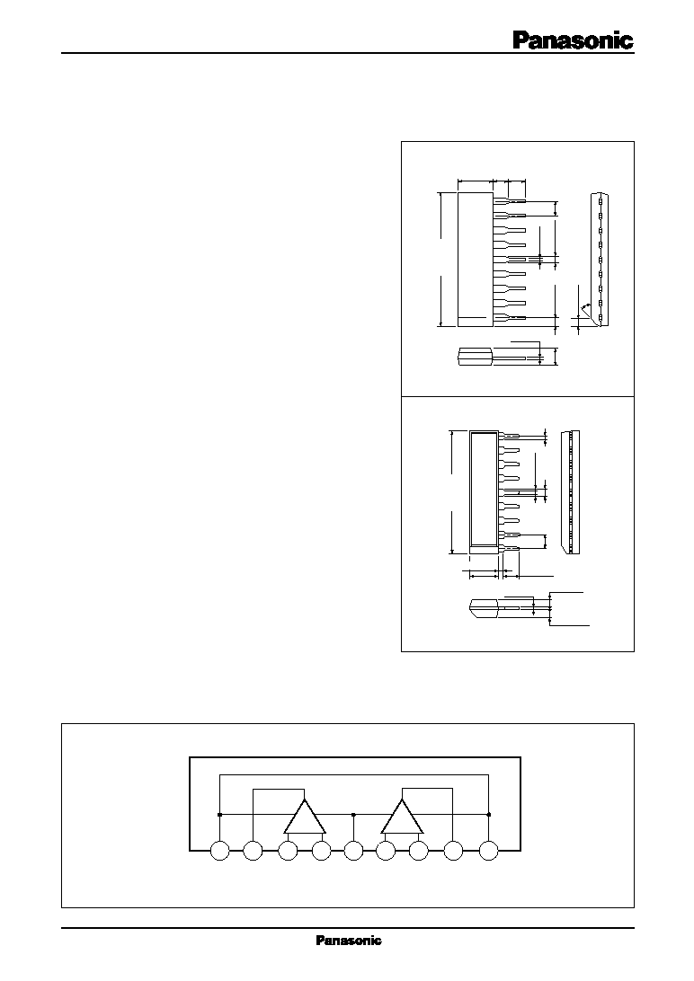
s Block Diagram
9
8
7
6
5
4
3
2
0.3
+ 0.1
≠ 0.05
23.3
±
0.3
6.0
±
0.3
2.4
±
0.25
3.3
±
0.25
1.5
±
0.25
0.5
±
0.1
2.54
1.5
±
0.25
1.4
±
0.3
30∞
3.0
±
0.3
Unit:mm
AN6561
1
9-pin SIL Plastic Package (SIP009-P-0000C)
Unit:mm
AN6561L
21.7
±
0.3
9
8
7
6
5
4
3
2
1
2.54
1.2
±
0.25
0.4
±
0.25
0.5
±
0.1
4.3
±
0.3
2.7
±
0.25
9-pin SIL Plastic Package (SIP009-P-0000A)
1.4
±
0.25
1.35
±
0.25
0.3
+0.1
≠ 0.05
1.0
±
0.25
+
≠
+
≠
V
CC
V
O1
V
CC
V
O2
+
V
in1
V
EE
1
1
2
2
3
4
5
6
8
7
9
≠
V
in1
≠
V
in2
+
V
in2
(GND)

s Pins Descriptions
Pin No.
Pin name
1
2
3
4
5
6
7
8
9
Positive supply voltage
Ch.1 output pin
Ch.1 inverting input pin
Ch.1 non-inverting input pin
Negative supply voltage (GND)
Ch.2 non-inverting input pin
Ch.2 inverting input pin
Ch.2 output pin
Positive supply voltage
V
CC
V
ID
V
ICM
V
O
P
D
T
opr
T
stg
Supply voltage
Differential input voltage
Common-mode input voltage
Output voltage
Power dissipation
Operating ambient temperature
Storage temperature
V
V
V
V
mW
∞C
∞C
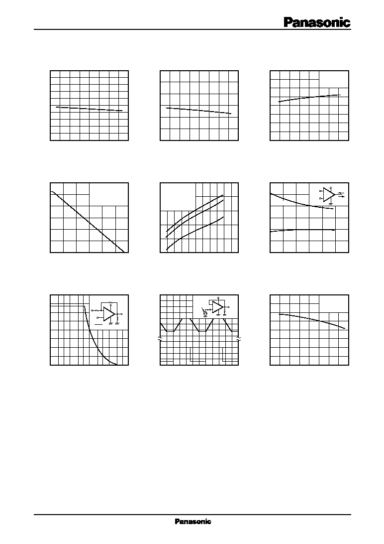
Parameter
Symbol
Rating
Unit
s Absolute Maximum Rating (Ta=25∞C)
32
32
≠ 0.3 to +32
24
350
≠20 to +75
≠55 to +150
Parameter
Symbol
Condition
min
typ
max
s Electrical Characteristics (V
CC
=5V, Ta=25∞C)
Input offset voltage
V
I (offset)
7
mV
2
R
S
=50
I
Bias
250
nA
Input bias current
Input offset current
I
IO
50
nA
Common-mode input voltage width
0
V
CM
V
Supply current
I
CC
mA
R
L
=
Voltage gain
G
V
dB
100
R
L
2k
Maximum output voltage
V
CC
≠1.5
V
O (max.)
V
R
L
2k
Common-mode rejection ratio
65
CMR
dB
85
Supply voltage rejection ratio
65
SVR
dB
100
Channel separation
CS
dB
120
f=1kHz to 20kHz
Output source current
I
O (source)
mA
40
V
in
+
=1V, V
in
≠
= 0V
V
CC
≠1.5
1.2
0.6
20
10
Output sink current
I
SINK
mA
20
V
in
+
= 0V, V
in
≠
=1V
Unit
=
>
=
>
Parameter
Symbol
Range
s Recommended Operating Range (Ta=25∞C)
Operating supply voltage range
V
CC
Single power supply 3V to 30V
Dual power supply
±
1.5V to
±
15V
+
≠
OP. Amp.
V
CC
V
O
V
in
R
2
R
1
Non-inverting amplifier
V
O
= 1+ Vin
R
2
R
1
s Application Circuit