ICs for Audio Common Use
s
Overview
The AN7149N is an integrated circuit designed for
power amplifier of 5.3W (12.0V, 3
) output. Stereo oper-
ation is enabled due to incorporating two amps. on one
chip. It makes high reliability by smaller quiescent current
compared with power amp. current and protectors built in.
As quiescent circuit current is very few, it is most suitably
used for battery operated set such as radio cassette
recorder. Furthermore, low distortion and low noise are
realized and external components are very few. 12-pin
SIL package enabled compact and high-densely mounted
set.
s
Features
∑
Low quiescent current
∑
High operation stability
∑
Low radiation
∑
Low distortion
∑
Low noise
∑
Low shock noise from power ON/OFF operation
∑
Fewer external components
AN7149N
Dual 5.3W Audio Power Amplifier Circuit
29.96
±
0.3
29.6
±
0.3
12
1
Unit : mm
28.0
±
0.3
20.0
±
0.2
5.9
±
0.25 7.7
±
0.3 7.8
±
0.25
1.2
±
0.1
2.54
0.6
±
0.1
3.5
±
0.3
0.35
+ 0.1
≠ 0.05
¯ 3.6
R1.8
0.6
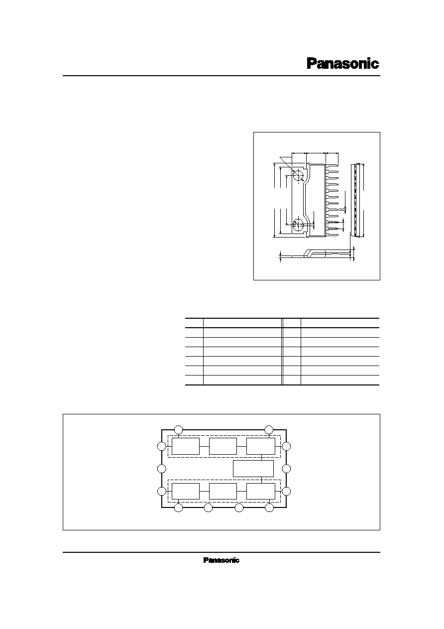
12-Lead SIP Package with Fin (HSIP012-P-0000A)
s
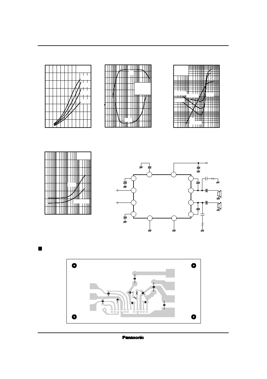
Block Diagram
Input
Circuit
Driver
Circuit
Output
Circuit
GND (Output)
GND (Input)
2
3
Input
Circuit
Driver
Circuit
Output
Circuit
5
6
4
9
8
12
10
7
1
11
V
CC
Over Current
Over Temperature
Protection
s
Pin Descriptions
Pin No.
Pin Name
1
2
3
4
5
6
N.F.B Ch.1
Input Ch.1
Ripple Filter
GND (Input)
Input Ch.2
N.F.B Ch.2
Pin No.
Pin Name
7
8
9
10
11
12
Output Ch.2
Bootstrap Ch.2
GND (Output)
V
CC
Bootstrap Ch.1
Output Ch.1
ICs for Audio Common Use
AN7149N
s
Absolute Maximum Ratings
(Ta= 25∞C)
V
CC
I
CC
P
D
T
opr
T
stg
Supply Voltage
Supply Current
Power Dissipation
Operating Ambient Temperature
Storage Temperature
V
A
W
∞C
∞C
Parameter
Symbol
Rating
Unit
24
4
41.7
≠ 30 ~ + 75
≠ 55 ~ + 150
V
i
= 0mV
P
O
= 1.0W
P
O
= 1.0W, f
= 1kHz
THD
= 10%, R
L
= 3
THD
= 10%, R
L
= 4
Parameter
Symbol
Condition
min.
typ.
max.
Unit
s
Electrical Characteristics
(V
CC
= 12V, R
C
= 3
, f
= 1kHz, Ta
= 25∞C)
Quiescent Circuit Current
Voltage Gain
Total Harmonic Distortion
I
CQ
G
V
THD
47.5
4.7
40
13
49.5
0.2
5.3
4.3
2.9
0.5
0
45
19
51.5
0.5
1.0
1.0
mA
dB
%
W
mV
dB
dB
R
g
= 10k
, f
= 15Hz ~ 30kHz,
12dB/OCT
P
O
= 0.5W
P
O
= 0.5W
Maximum Output Power
Output Noise Voltage
Channel Balance
Ripple Rejection Ratio
V
no
CB
RR
P
O
THD
= 10%, V
CC
= 9V,
R
L
= 3
P
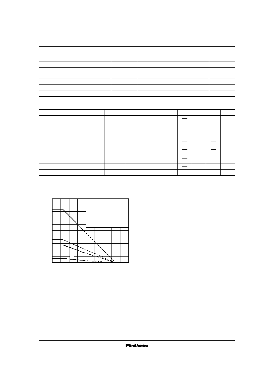
D
≠ Ta
50
40
30
20
10
0
Ambient Temperature Ta (∞C)
P
o
w
e
r
D
i
s
s
i
p
a
t
i
o
n
P
D
(
W
)
120
0
40
80
(4)
160
(3)
(2)
(1)
(1) Tc = Ta (
j≠ c = 3∞C/W)
(2) With a 100cm
2
◊
3mm Al
heat sink (black color coated)
or a 200cm
2
◊
2mm Al heat
sink (not lacquered)
(3) With a 100cm
2
◊
2mm Al
heat sink (not lacquered)
(4) Without heat sink