 | –≠–ª–µ–∫—Ç—Ä–æ–Ω–Ω—ã–π –∫–æ–º–ø–æ–Ω–µ–Ω—Ç: AN7261FBQ | –°–∫–∞—á–∞—Ç—å:  PDF PDF  ZIP ZIP |
ICs for FM/AM Tuner
1
AN7261FBQ
FM multiplex reception IC
s
Overview
The AN7261FBQ is an FM-multiplex reception IC
including a front-end and an IF block for FM tuner. Since
the receiving circuit of FM multiplex signal is integrated
on a single chip, it is most suitable for saving the space of
sets.
s
Features
∑
A single chip IC for an FM-multiplex tuner block, which
was conventionally composed of two ICs.
∑
Fewer external components
∑
Can be used for 15 MHz IF
s
Applications
∑
VICS, RDS
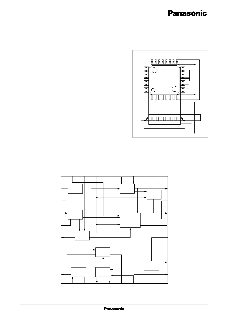
LQFP032-P-0707
Unit : mm
7.0±0.3
(0.55)
1.4±0.2
0.625±0.100
0.625±0.100
0.1±0.1
9.2±0.4
7.0±0.3
0.8
9.2±0.4
0.3
+0.10
≠0.05
0.15
+0.10
≠0.05
1
8
24
17
9
16
32
25
s
Block Diagram
25
V
REF
V
REF
26
GND1
27
28
29
V
C
30
31
32
16
AFC
15
SD adj.
14
Det.
13
12
11
GND2
10
OSC
9
AGC
1
2
3
4
5
ADX
6
RF in
7
V
CC2
8
N.C.
24
Band
23
V
C
adj.
22
21
Mute adj.
20
19
18
V
CC1
17
Mute
IF
det.
Mix.
OSC
AGC
amp.
IF
amp.
Band det.
SD
IF counter
IF
limiter
Level
det.
AN7261FBQ
ICs for FM/AM Tuner
2
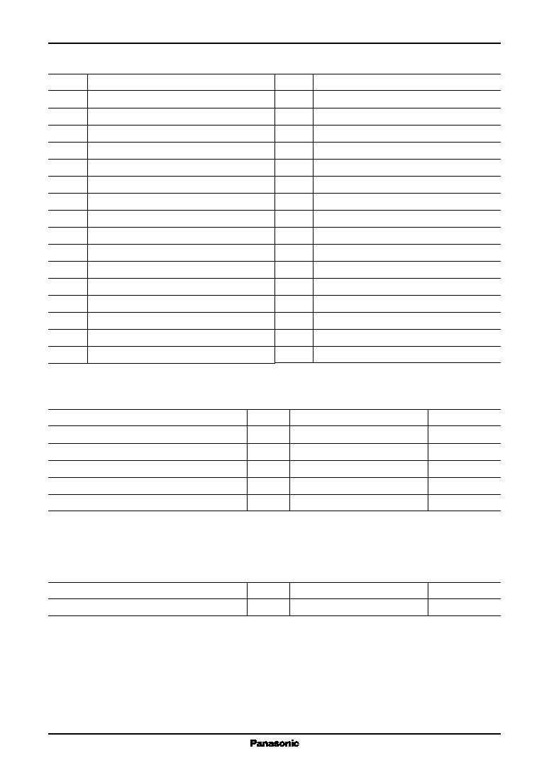
Parameter
Symbol
Rating
Unit
Supply voltage
V
CC
9.1
V
Supply current
I
CC
66
mA
Power dissipation
*2
P
D
343.6
mW
Operating ambient temperature
*1
T
opr
-
30 to
+
80
∞
C
Storage temperature
*1
T
stg
-
55 to
+
150
∞
C
Parameter
Symbol
Range
Unit
Supply voltage
V
CC
7.2 to 9.0
V
s
Recommended Operating Range
s
Pin Descriptions
Pin No.
Description
1
1st IF input
2
GND for 1st IF input
3
Mixer output 1
4
Mixer output 2
5
PIN diode driver
6
Mix. Input
7
V
CC2
8
N.C.
9
AGC output
10
OSC buffer output
11
GND2
12
OSC
13
SD/IF counter output
14
Detection output
15
SD sensitivity adjustment
16
AFC voltage output
Pin No.
Description
17
Higher freguency correction adjustment
18
V
CC1
19
FM detection
20
2nd IF output
21
Mute adjustment
22
Mute voltage output
23
Control voltage adjustment
24
Band mute SW/band signal output
25
V
REF
26
GND1
27
2nd IF input
28
GND for 2nd IF input
29
Control voltage output
30
Keyed-AGC input
31
AGC sensitivity adjustment
32
1st IF output
Note) *1: T
a
=
25
∞
C except power dissipation, operating ambient temperature and storage temperature.
*2: T
a
=
80
∞
C
s
Absolute Maximum Ratings
ICs for FM/AM Tuner
AN7261FBQ
3
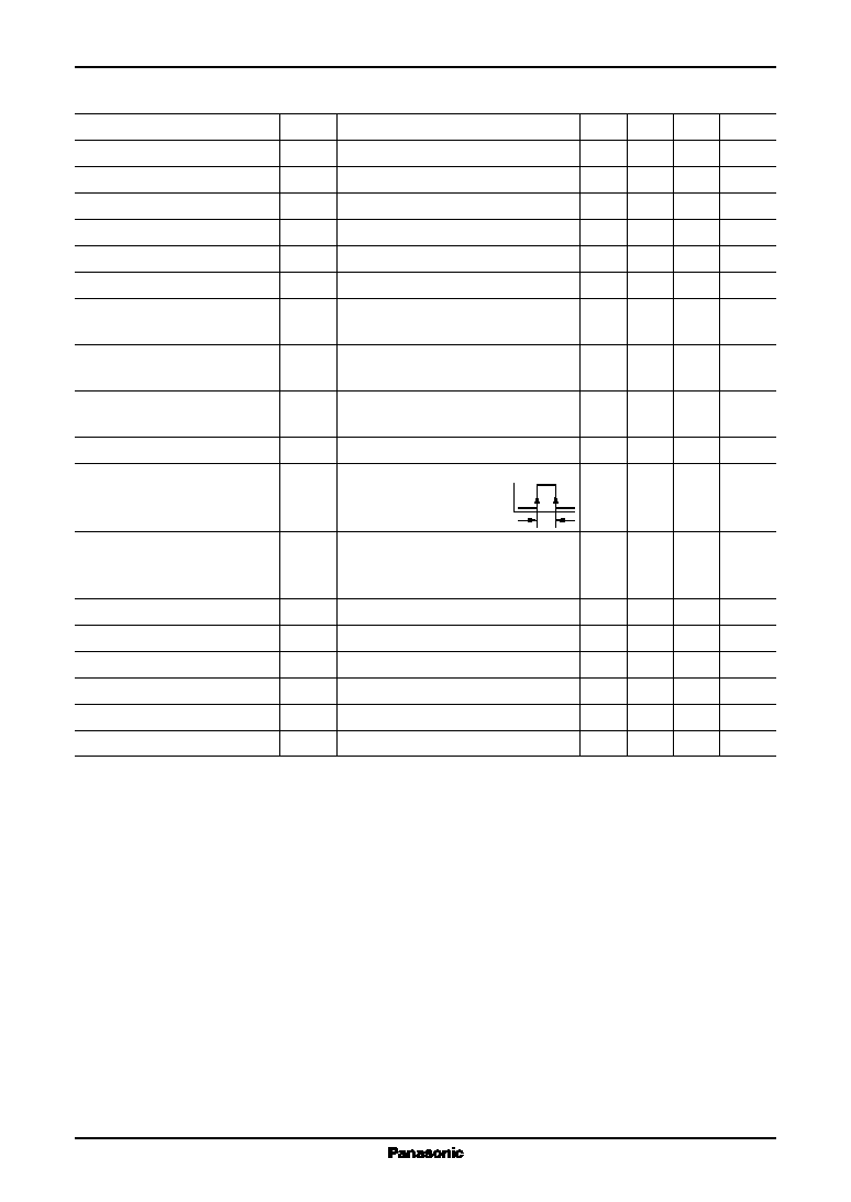
s
Electrical Characteristics at V
CC
=
8 V, f
IN1
=
98 MHz, f
IN2
=
15 MHz, T
a
=
25
∞
C
Parameter
Symbol
Conditions
Min
Typ
Max
Unit
Control voltage 1
V
C1
No signal input, DC voltage of pin 29
0.0
0.05
0.8
V
Control voltage 2
V
C2
V
IN2
=
60 dB
µ
, DC voltage of pin 29
0.7
1.25
1.8
V
Control voltage 3
V
C3
V
IN2
=
80 dB
µ
, DC voltage of pin 29
1.8
2.4
3.0
V
Control voltage 4
V
C4
V
IN2
=
100 dB
µ
, DC voltage of pin 29
3.0
3.7
4.4
V
Control voltage 5
V
C5
V
C5
=
V
C3
-
V
C2
1.0
1.2
1.4
V
Control voltage 6
V
C6
V
C6
=
V
C4
-
V
C3
1.05
1.25
1.45
V
Detection output level 1
V
O1
V
IN2
=
80 dB
µ
/1 kHz, 30%FM,
70
90
110
mV[rms]
AC voltage of pin 14
Detection output level 2
V
O2
V
IN2
=
80 dB
µ
/76 kHz, 10%FM,
37
47
57
mV[rms]
AC voltage of pin 14
Counter output level
V
IFC
V
IN2
=
100 dB
µ
, V
15
=
2 V,
150
180
210
mV[rms]
IFC output level
SD sensitivity
SD
S
V
IN2
when V
15
=
2 V, SD
>
4 V
61
71
81
dB
µ
SD bandwidth
SD
W
Bandwidth when SD
>
4 V,
90
115
140
kHz
V
IN2
=
100 dB
µ
Limiting sensitivity
V
LIM
V
IN2
level, 30 kHz LPF on, and 1 kHz
40
48
54
dB
µ
30% FM when pin 14 AC voltage
drops by 3 dB
Local oscillation buffer output
V
OS
f
OSC
=
113 MHz, without input
110
160
210
mV[rms]
IF output level
V
IF
V
IN1
=
80 dB
µ
, IF out level
60
110
170
mV[rms]
AGC sensitivity
S
AGC
V
IN1
level when V
9
=
3 V
68
72
76
dB
µ
High-level AGC voltage
V
AH
V
IN1
=
66 dB
µ
, V
9
5.9
6.3
6.7
V
Low-level AGC voltage
V
AL
V
IN1
=
78 dB
µ
, V
9
0.05
0.5
V
Supply current
I
TOT
Without input
41
52
65
mA
Note) FM tuning condition: Adjust the V
T
of application voltage so that OSC buffer output frequency becomes 113 MHz
±
10 kHz.
SD
s
Usage Notes
1. Use less than 10 k
of external resistor of pin 31
2. Use this IC not to exceed allowable power dissipation value refering to the "s Technical Information".
AN7261FBQ
ICs for FM/AM Tuner
4
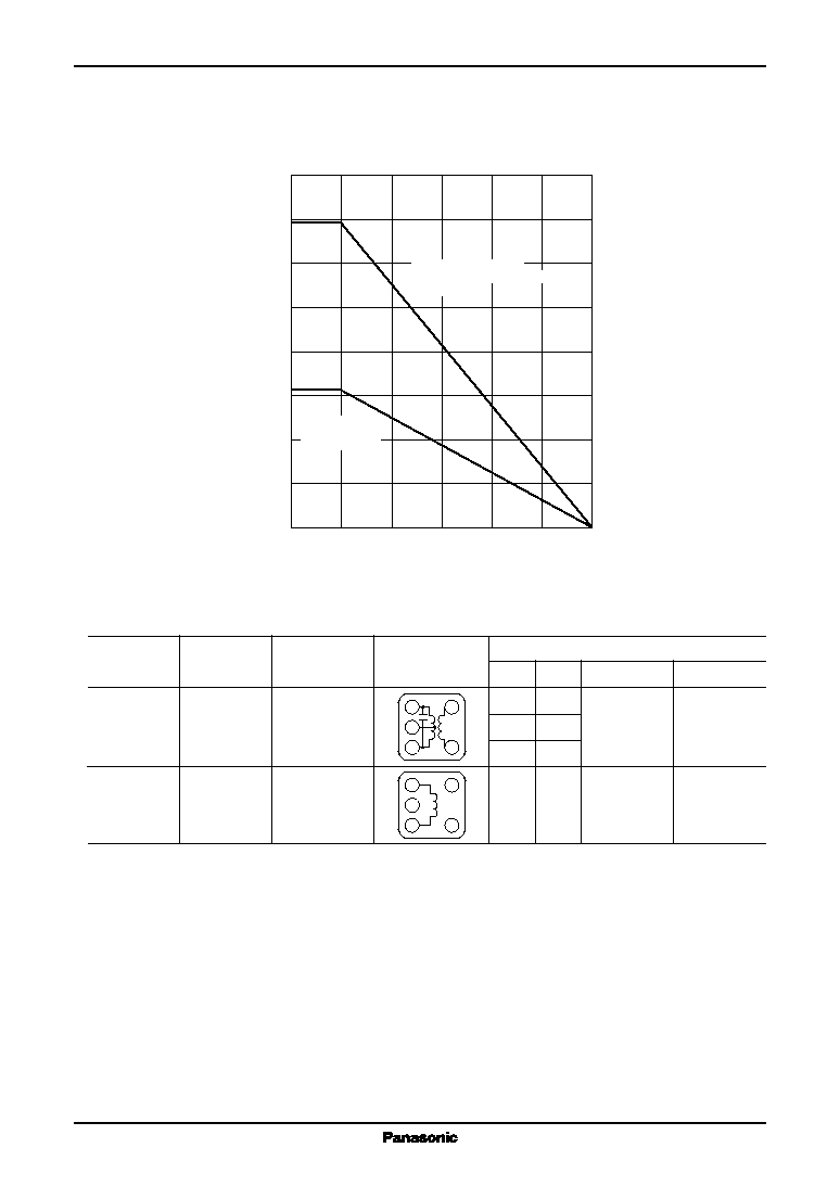
2. Specification for special parts
Part
Maker
Maker
Connection
Specification
part number
Pin No. Turns
LC value
Q at no load
IF coil
Sumida
4162-T006
4-6
10T
12 pF
±
10%
50 or more
1-2
11T
(15 MHz)
2-3
11T
Detection
Matsushita
SQF5EB033A
1-3
11T
0.59
µ
H
41
±
20%
coil
electronics
±
5.0%
(15 MHz)
parts
3
2
1
4
6
3
2
1
4
6
s
Technical Information
1. P
D
T
a
curves of LQFP032-P-0707
P
D
T
a
1.200
1.000
1.600
1.388
1.400
0.800
0.600
0.400
0.200
0.613
0.000
0
25
50
Independent IC
without heat shink
R
th(j-a)
=
203.7
∞
C/W
Mounted on standard board
(grass epoxy : 50 mm
◊
50 mm
◊
t0.8 mm)
R
th(j-a)
=
90.0
∞
C/W
75
100
125
150
Ambient temperature T
a
(∞
C)
Po
wer dissipation P
D
(W)
ICs for FM/AM Tuner
AN7261FBQ
5
s
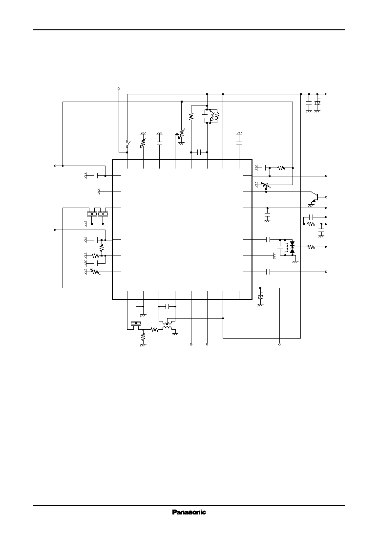
Application Circuit Example
25
V
REF
26
GND1
27
28
29
V
C
30
31
32
16
15
SD adj.
100 k
51 k
1
µ
F 3.9 k
300
14
13
12
11 GND2
10
OSC
VT
SD
IFC
1
µ
F
1000 pF
1000 pF
1000 pF
27 pF 3 pF
9
1
2
3
4
5
ADX
6
RF in
AG
C
7
V
CC2
8
N.C.
24
23
V
C
adj.
Band
22
21
Mute adj.
20
19
18
V
CC1
17
Det.
Seek
AFC
V
CC
470
330
1000 pF
100 pF
0.1
µ
F
18 pF
100
µ
F
0.1
µ
F
180 pF
2.2 k
100 k
50 k
0.1
µ
F
50 k
100 k
10 k
0.01
µ
F
0.01
µ
F