 | –≠–ª–µ–∫—Ç—Ä–æ–Ω–Ω—ã–π –∫–æ–º–ø–æ–Ω–µ–Ω—Ç: AN79LXXM | –°–∫–∞—á–∞—Ç—å:  PDF PDF  ZIP ZIP |
Voltage Regulators
1
Publication date: December 2001
SFF00006CEB
AN79Lxx/AN79LxxM Series
3-pin negative output voltage regulator (100 mA type)
I Overview
The AN79Lxx series and the AN79LxxM series are
3-pin, fixed negative output type monolithic voltage
regulators.
Stabilized fixed output voltage is obtained from un-
stable DC input voltage without using any external compo-
nents. 12 types of output voltage are available:
-4V, -5V,
-6V, -7V, -8V, -9V, -10V, -12V, -15V, -18V, -20V
and
-24V. They can be used widely in power circuits with
current capacity of up to 100mA.
I Features
∑ No external components
∑ Output voltage: -4V, -5V, -6V, -7V, -8V, -9V,-10V,
-12V, -15V, -18V, -20V, -24V
∑ Built-in overcurrent limit circuit
∑ Built-in thermal overload protection circuit
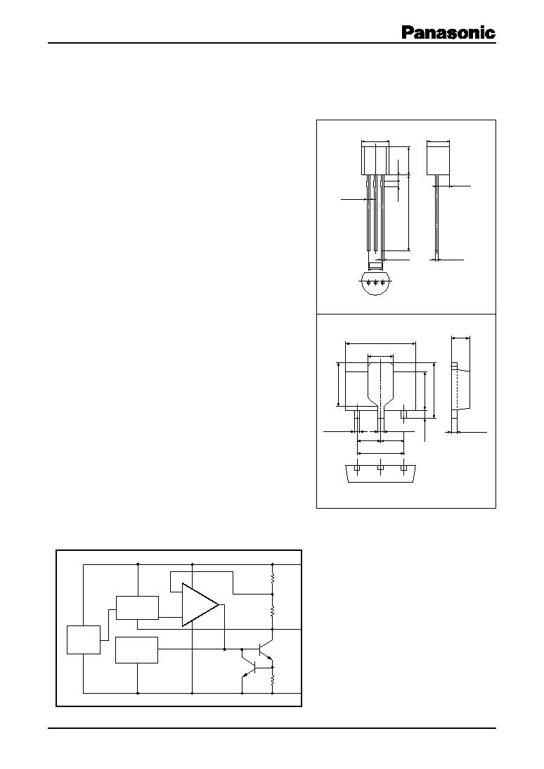
SSIP003-P-0000
AN79Lxx series
Unit: mm
HSIP003-P-0000B
AN79LxxM series
Unit: mm
5.0±0.2
5.1±0.2
13.5±0.5
(1.0)
(1.0)
4.0±0.2
2.3±0.2
0.6±0.15
0.43
+0.1
≠0.05
2.54
0.43
+0.1
≠0.05
2
1
3
2.6 typ.
1.6 max.
1.8 max.
4.6 max.
3.0
1.5
1.5
3
2
1
0.48 max.
0.58 max.
0.44 max.
4.25 max.
2.6 max.
0.8 min.
I Block Diagram (AN79Lxx series)
2
1
3
Common
(1)
Output
(3)
Input
(2)
Starter
Voltage
Reference
Error Amp.
+
-
R
1
Q
1
Pass Tr.
R
SC
Current
Limiter
Thermal
Protection
R
2
Note) The number in ( ) shows the pin number for the AN79LxxM series.
1 : Common
2 : Input
3 : Output
1 : Output
2 : Common
3 : Intput
Note) The packages (SSIP003-P-0000 and HSIP003-
P-0000B) of this product will be changed to
lead-free type (SSIP003-P-0000S and
HSIP003-P-0000Q). See the new package di-
mensions section later of this datasheet.

AN79Lxx/AN79LxxM Series
2
SFF00006CEB
I Absolute Maximum Ratings at T
a
= 25∞C
I Electrical Characteristics at T
a
= 25∞C
∑ AN79L04 (-4V type)
V
I
P
D
T
opr
T
stg
V
V
mW
∞C
∞C
Parameter
Symbol
Rating
Unit
-35 *
1
-40 *
2
650 *
3
-20 to +80
-55 to +150
-55 to +125
Input voltage
Power dissipation
Operating ambient temperature
Storage temperature
AN79Lxx series
AN79LxxM series
*1 AN79L04, AN79L05/M, AN79L06, AN79L07, AN79L08/M, AN79L09/M, AN79L10, AN79L12/M, AN79L15/M, AN79L18
*2 AN79L20, AN79L24
*3 Follow the derating curve. When T
j
exceeds 150
∞C, the internal circuit cuts off the output.
AN79LxxM series is mounted on a standard board (glass epoxy: 20mm
◊ 20mm ◊ t1.7mm with Cu foil of 1cm
2
or more).
Parameter
Symbol
Conditions
Min
Typ
Max
Output voltage
V
O
V
T
j
= 25∞C
Output voltage tolerance
V
O
V
V
I
= -7 to -19V, I
O
= 1 to 70mA
Line regulation
REG
IN
mV
V
I
= -6 to -20V, T
j
= 25∞C
mV
Load regulation
REG
L
mV
I
O
= 1 to 100mA, T
j
= 25∞C
mV
I
O
= 1 to 40mA, T
j
= 25∞C
V
I
= -7 to -17V, T
j
= 25∞C
mA
T
j
= 25∞C
Note 1) The specified condition T
j
= 25∞C means that the test should be carried out within so short a test time (within 10ms) that the
characteristic value drift due to the chip junction temperature rise can be ignored.
Note 2) Unless otherwise specified, V
I
= -9V, I
O
= 40mA, C
I
= 2µF, C
O
= 1µF, T
j
= 0 to 125∞C
Bias current
I
Bias
mA
V
I
= -7 to -19V, T
j
= 25∞C
Bias current fluctuation to input
I
Bias(IN)
mA
Bias current fluctuation to load
I
Bias(L)
µV
I
O
= 1 to 40mA, T
j
= 25∞C
Output noise voltage
V
no
dB
f
= 10Hz to 100kHz, T
a
= 25∞C
Ripple rejection ratio
RR
V
I
= -7 to -17V, f = 120Hz, T
a
= 25∞C
V
T
j
= 25∞C
Minimum input/output voltage difference
V
DIF(min)
mA
Output short-circuit current
I
O(Short)
mV/
∞C
V
I
= -35V, T
j
= 25∞C
Output voltage temperature coefficient
V
O
/T
a
I
O
= 5mA
Unit
-4.16
-4
80
10
3
38
0.5
0.1
40
-4.2
60
30
5
55
-3.84
-3.8
0.8
200
- 0.4
4.5
AN79Lxx/AN79LxxM Series
3
SFF00006CEB
I Electrical Characteristics at T
a
= 25∞C (continued)
∑ AN79L05, AN79L05M (-5V type)
∑ AN79L06 (-6V type)
V
O
V
T
j
= 25∞C
V
O
V
V
I
= -9 to -21V, I
O
= 1 to 70mA
REG
IN
mV
V
I
= -8 to -22V, T
j
= 25∞C
mV
REG
L
mV
I
O
= 1 to 100mA, T
j
= 25∞C
mV
I
O
= 1 to 40mA, T
j
= 25∞C
V
I
= -9 to -19V, T
j
= 25∞C
mA
T
j
= 25∞C
I
Bias
mA
V
I
= -9 to -21V, T
j
= 25∞C
I
Bias(IN)
mA
I
Bias(L)
µV
I
O
= 1 to 40mA, T
j
= 25∞C
V
no
dB
f
= 10Hz to 100kHz, T
a
= 25∞C
RR
V
I
= -9 to -19V, f = 120Hz, T
a
= 25∞C
V
T
j
= 25∞C
V
DIF(min)
mA
I
O(Short)
mV/
∞C
V
I
= -35V, T
j
= 25∞C
V
O
/T
a
I
O
= 5mA
-6.24
-6
120
12
3
44
0.5
0.1
60
-6.3
60
30
5
55
-5.76
-5.7
0.8
200
- 0.4
5.5
Parameter
Symbol
Conditions
Min
Typ
Max
Output voltage
Output voltage tolerance
Line regulation
Load regulation
Note 1) The specified condition T
j
= 25∞C means that the test should be carried out within so short a test time (within 10ms) that the
characteristic value drift due to the chip junction temperature rise can be ignored.
Note 2) Unless otherwise specified, V
I
= -11V, I
O
= 40mA, C
I
= 2µF, C
O
= 1µF, T
j
= 0 to 125∞C
Bias current
Bias current fluctuation to input
Bias current fluctuation to load
Output noise voltage
Ripple rejection ratio
Minimum input/output voltage difference
Output short-circuit current
Output voltage temperature coefficient
Unit
V
O
V
T
j
= 25∞C
V
O
V
V
I
= -8 to -20V, I
O
= 1 to 70mA
REG
IN
mV
V
I
= -7 to -21V, T
j
= 25∞C
mV
REG
L
mV
I
O
= 1 to 100mA, T
j
= 25∞C
mV
I
O
= 1 to 40mA, T
j
= 25∞C
V
I
= -8 to -18V, T
j
= 25∞C
mA
T
j
= 25∞C
I
Bias
mA
V
I
= -8 to -20V, T
j
= 25∞C
I
Bias(IN)
mA
I
Bias(L)
µV
I
O
= 1 to 40mA, T
j
= 25∞C
V
no
dB
f
= 10Hz to 100kHz, T
a
= 25∞C
-4.8
RR
V
I
= -8 to -18V, f = 120Hz, T
a
= 25∞C
V
T
j
= 25∞C
V
DIF(min)
mA
I
O(Short)
mV/
∞C
V
I
= -35V, T
j
= 25∞C
V
O
/T
a
I
O
= 5mA
-5.2
-5
100
11
3
40
0.5
0.1
50
-5.25
60
30
5
55
-4.75
0.8
200
- 0.4
5
Parameter
Symbol
Conditions
Min
Typ
Max
Output voltage
Output voltage tolerance
Line regulation
Load regulation
Note 1) The specified condition T
j
= 25∞C means that the test should be carried out within so short a test time (within 10ms) that the
characteristic value drift due to the chip junction temperature rise can be ignored.
Note 2) Unless otherwise specified, V
I
= -10V, I
O
= 40mA, C
I
= 2µF, C
O
= 1µF, T
j
= 0 to 125∞C (AN79L05) and T
j
= 0 to 100∞C
(AN79L05M)
Bias current
Bias current fluctuation to input
Bias current fluctuation to load
Output noise voltage
Ripple rejection ratio
Minimum input/output voltage difference
Output short-circuit current
Output voltage temperature coefficient
Unit

AN79Lxx/AN79LxxM Series
4
SFF00006CEB
I Electrical Characteristics at T
a
= 25∞C (continued)
∑ AN79L07 (-7V type)
∑ AN79L08, AN79L08M (-8V type)
V
O
V
T
j
= 25∞C
V
O
V
V
I
= -11 to -23V, I
O
= 1 to 70mA
REG
IN
mV
V
I
= -10 to -24V, T
j
= 25∞C
mV
REG
L
mV
I
O
= 1 to 100mA, T
j
= 25∞C
mV
I
O
= 1 to 40mA, T
j
= 25∞C
V
I
= -11 to -21V, T
j
= 25∞C
mA
T
j
= 25∞C
I
Bias
mA
V
I
= -11 to -23V, T
j
= 25∞C
I
Bias(IN)
mA
I
Bias(L)
µV
I
O
= 1 to 40mA, T
j
= 25∞C
V
no
dB
f
= 10Hz to 100kHz, T
a
= 25∞C
RR
V
I
= -11 to -21V, f = 120Hz, T
a
= 25∞C
V
T
j
= 25∞C
V
DIF(min)
mA
I
O(Short)
mV/
∞C
V
I
= -35V, T
j
= 25∞C
V
O
/T
a
I
O
= 5mA, T
j
= 0 to 125∞C
-8.32
-8
160
15
3
52
0.5
0.1
80
-8.4
80
40
5
54
-7.68
-7.6
0.8
200
- 0.6
7
Parameter
Symbol
Conditions
Min
Typ
Max
Output voltage
Output voltage tolerance
Line regulation
Load regulation
Note 1) The specified condition T
j
= 25∞C means that the test should be carried out within so short a test time (within 10ms) that the
characteristic value drift due to the chip junction temperature rise can be ignored.
Note 2) Unless otherwise specified, V
I
= -14V, I
O
= 40mA, C
I
= 2µF, C
O
= 1µF, T
j
= 0 to 125∞C (AN79L08) and T
j
= 0 to 100∞C
(AN79L08M)
Bias current
Bias current fluctuation to input
Bias current fluctuation to load
Output noise voltage
Ripple rejection ratio
Minimum input/output voltage difference
Output short-circuit current
Output voltage temperature coefficient
Unit
V
O
V
T
j
= 25∞C
V
O
V
V
I
= -10 to -22V, I
O
= 1 to 70mA
REG
IN
mV
V
I
= -9 to -23V, T
j
= 25∞C
mV
REG
L
mV
I
O
= 1 to 100mA, T
j
= 25∞C
mV
I
O
= 1 to 40mA, T
j
= 25∞C
V
I
= -10 to -20V, T
j
= 25∞C
mA
T
j
= 25∞C
I
Bias
mA
V
I
= -10 to -22V, T
j
= 25∞C
I
Bias(IN)
mA
I
Bias(L)
µV
I
O
= 1 to 40mA, T
j
= 25∞C
V
no
dB
f
= 10Hz to 100kHz, T
a
= 25∞C
RR
V
I
= -10 to -20V, f = 120Hz, T
a
= 25∞C
V
T
j
= 25∞C
V
DIF(min)
mA
I
O(Short)
mV/
∞C
V
I
= -35V, T
j
= 25∞C
V
O
/T
a
I
O
= 5mA
-7.28
-7
140
13
3
48
0.5
0.1
70
-7.35
70
40
5
54
-6.72
-6.65
0.8
200
- 0.5
6
Parameter
Symbol
Conditions
Min
Typ
Max
Output voltage
Output voltage tolerance
Line regulation
Load regulation
Note 1) The specified condition T
j
= 25∞C means that the test should be carried out within so short a test time (within 10ms) that the
characteristic value drift due to the chip junction temperature rise can be ignored.
Note 2) Unless otherwise specified, V
I
= -12V, I
O
= 40mA, C
I
= 2µF, C
O
= 1µF, T
j
= 0 to 125∞C
Bias current
Bias current fluctuation to input
Bias current fluctuation to load
Output noise voltage
Ripple rejection ratio
Minimum input/output voltage difference
Output short-circuit current
Output voltage temperature coefficient
Unit

AN79Lxx/AN79LxxM Series
5
SFF00006CEB
I Electrical Characteristics at T
a
= 25∞C (continued)
∑ AN79L09, AN79L09M (-9V type)
∑ AN79L10 (-10V type)
V
O
V
T
j
= 25∞C
V
O
V
V
I
= -13 to -25V, I
O
= 1 to 70mA
REG
IN
mV
V
I
= -12 to -26V, T
j
= 25∞C
mV
REG
L
mV
I
O
= 1 to 100mA, T
j
= 25∞C
mV
I
O
= 1 to 40mA, T
j
= 25∞C
V
I
= -13 to -23V, T
j
= 25∞C
mA
T
j
= 25∞C
I
Bias
mA
V
I
= -13 to -25V, T
j
= 25∞C
I
Bias(IN)
mA
I
Bias(L)
µV
I
O
= 1 to 40mA, T
j
= 25∞C
V
no
dB
f
= 10Hz to 100kHz, T
a
= 25∞C
RR
V
I
= -13 to -23V, f = 120Hz, T
a
= 25∞C
V
T
j
= 25∞C
V
DIF(min)
mA
I
O(Short)
mV/
∞C
V
I
= -35V, T
j
= 25∞C
V
O
/T
a
I
O
= 5mA
-10.4
-10
160
17
3
65
0.5
0.1
80
-10.5
100
50
5
53
-9.6
-9.5
0.8
200
- 0.7
9
Parameter
Symbol
Conditions
Min
Typ
Max
Output voltage
Output voltage tolerance
Line regulation
Load regulation
Note 1) The specified condition T
j
= 25∞C means that the test should be carried out within so short a test time (within 10ms) that the
characteristic value drift due to the chip junction temperature rise can be ignored.
Note 2) Unless otherwise specified, V
I
= -16V, I
O
= 40mA, C
I
= 2µF, C
O
= 1µF, T
j
= 0 to 125∞C
Bias current
Bias current fluctuation to input
Bias current fluctuation to load
Output noise voltage
Ripple rejection ratio
Minimum input/output voltage difference
Output short-circuit current
Output voltage temperature coefficient
Unit
V
O
V
T
j
= 25∞C
V
O
V
V
I
= -12 to -24V, I
O
= 1 to 70mA
REG
IN
mV
V
I
= -11 to -25V, T
j
= 25∞C
mV
REG
L
mV
I
O
= 1 to 100mA, T
j
= 25∞C
mV
I
O
= 1 to 40mA, T
j
= 25∞C
V
I
= -12 to -22V, T
j
= 25∞C
mA
T
j
= 25∞C
I
Bias
mA
V
I
= -12 to -24V, T
j
= 25∞C
I
Bias(IN)
mA
I
Bias(L)
µV
I
O
= 1 to 40mA, T
j
= 25∞C
V
no
dB
f
= 10Hz to 100kHz, T
a
= 25∞C
RR
V
I
= -12 to -22V, f = 120Hz, T
a
= 25∞C
V
T
j
= 25∞C
V
DIF(min)
mA
I
O(Short)
mV/
∞C
V
I
= -35V, T
j
= 25∞C
V
O
/T
a
I
O
= 5mA, T
j
= 0 to 125∞C
-9.36
-9
160
16
3
58
0.5
0.1
80
-9.45
90
50
5
53
-8.64
-8.55
0.8
200
- 0.6
8
Parameter
Symbol
Conditions
Min
Typ
Max
Output voltage
Output voltage tolerance
Line regulation
Load regulation
Note 1) The specified condition T
j
= 25∞C means that the test should be carried out within so short a test time (within 10ms) that the
characteristic value drift due to the chip junction temperature rise can be ignored.
Note 2) Unless otherwise specified, V
I
= -15V, I
O
= 40mA, C
I
= 2µF, C
O
= 1µF, T
j
= 0 to 125∞C (AN79L09) and T
j
= 0 to 100∞C
(AN79L09M)
Bias current
Bias current fluctuation to input
Bias current fluctuation to load
Output noise voltage
Ripple rejection ratio
Minimum input/output voltage difference
Output short-circuit current
Output voltage temperature coefficient
Unit