 | ÐлекÑÑоннÑй компоненÑ: AN8000MS | СкаÑаÑÑ:  PDF PDF  ZIP ZIP |
AN8000MS
Voltage Regulators
1
Publication date: February 2002
SDH00013DEB
AN8000MS
Ripple filter IC for cellular phones
s Overview
The AN8000MS is a ripple filter IC that rejects the
ripple component superimposed on the regulator output.
Use for the VCO bias of cellular phones improves C/N
and S/N and makes the high-quality telephone commu-
nication possible. Furthermore, by decreasing the differ-
ence between I/O voltages, drop in the power supply volt-
age of VCO is reduced.
s Features
·
The I/O drop voltage is reduced to 0.3 V (A PNP tran-
sistor is used for the pass transistor)
·
The mounting area is reduced by adopting the mini-type
6-pin package
s Applications
·
Cellular phones and others
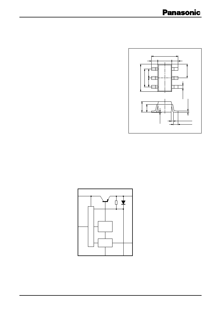
MINI-6D
Unit: mm
s Block Diagram
4
VIN
On/Off
1
VOUT
C2
6
2
3
5
C1
GND
Constant
current
Switch
V
oltage control
2.80
+0.20
0.30
1.50
(0.65)
(0.65)
6
5
4
1
2
3
(1.45)
(0.95)
(0.95)
1.90±0.20
+0.25
0.05
0.30
+0.10 0.05
2.90
+0.20 0.05
1.10
+0.20 0.10
(0.80)
0 to 0.10
0.16
+0.10 0.06
0.40±0.20
0.1 to 0.30
AN8000MS
2
SDH00013DEB
s Pin Descriptions
Pin No.
Symbol
Description
1
VIN
Input pin
2
C2
Capacitor connection pin 2
3
C1
Capacitor connection pin 1
4
VOUT
Output pin
5
GND
Ground pin
6
On/Off
Control pin
Note) *1: Except for the operating ambient temperature and storage temperature, all ratings are for T
a
=
25
°
C.
*2: The power dissipation shown is the value for T
a
=
75
°
C.
s Absolute Maximum Ratings
Parameter
Symbol
Rating
Unit
Supply voltage
V
IN
7.0
V
Supply current
I
IN
20
mA
Output current
I
O
-
15
mA
Allowable application voltage for
V
ON/OFF
V
IN
V
on/off pin
Allowable maximum capacitance for C1 pin
C
1
100
µ
F
Allowable maximum capacitance for C2 pin
C
2
10
µ
F
Power dissipation
*2
P
D
60
mW
Operating ambient temperature
*1
T
opr
-
25 to
+
75
°
C
Storage temperature
*1
T
stg
-
40 to
+
125
°
C
s Recommended Operating Range
Parameter
Symbol
Range
Unit
Supply voltage
V
CC
2.5 to 6.5
V
s Electrical Characteristics at T
a
=
25
°
C
Parameter
Symbol
Conditions
Min
Typ
Max
Unit
Output voltage 1
V
O1
V
IN
=
2.5 V, I
OUT
= -
1
µ
A
2.10
2.27
V
Output voltage 2
V
O2
V
IN
=
2.5 V, I
OUT
= -
15 mA
1.95
2.14
V
Output voltage 3
V
O3
V
IN
=
3.0 V, I
OUT
= -
1
µ
A
2.60
2.79
V
Output voltage 4
V
O4
V
IN
=
3.0 V, I
OUT
= -
15 mA
2.60
2.66
V
Output voltage 5
V
O5
V
IN
=
7.0 V, I
OUT
= -
1
µ
A
6.70
6.87
V
Output voltage 6
V
O6
V
IN
=
7.0 V, I
OUT
= -
15 mA
6.60
6.74
V
AN8000MS
3
SDH00013DEB
s Electrical Characteristics at T
a
=
25
°
C (continued)
Parameter
Symbol
Conditions
Min
Typ
Max
Unit
Consumption current 1
I
O1
V
IN
=
2.5 V, I
OUT
= -
1
µ
A
-
420
-
322
µ
A
Consumption current 2
I
O2
V
IN
=
2.5 V, I
OUT
= -
15 mA
-
400
-
304
µ
A
Consumption current 3
I
O3
V
IN
=
3.0 V, I
OUT
= -
1
µ
A
-
600
-
490
µ
A
Consumption current 4
I
O4
V
IN
=
3.0 V, I
OUT
= -
15 mA
-
550
-
450
µ
A
Consumption current 5
I
O5
V
IN
=
7.0 V, I
OUT
= -
1
µ
A
-
2.0
-
1.5
mA
Consumption current 6
I
O6
V
IN
=
7.0 V, I
OUT
= -
15 mA
-
2.0
-
1.7
mA
Load regulation 1
REG
L1
V
IN
=
2.5 V, I
OUT
= -
1
µ
A to
-
15 mA
0
134
200
mV
Load regulation 2
REG
L2
V
IN
=
3.0 V, I
OUT
= -
1
µ
A to
-
15 mA
0
122
200
mV
Load regulation 3
REG
L3
V
IN
=
7.0 V, I
OUT
= -
1
µ
A to
-
15 mA
0
126
200
mV
Consumption current against
I
REG1
V
IN
=
2.5 V, I
OUT
= -
1
µ
A to
-
15 mA
-
100
-
18
100
µ
A
load change 1
Consumption current against
I
REG2
V
IN
=
3.0 V, I
OUT
= -
1
µ
A to
-
15 mA
-
100
-
18
100
µ
A
load change 2
Consumption current against
I
REG3
V
IN
=
7.0 V, I
OUT
= -
1
µ
A to
-
15 mA
-
150
-
5
150
µ
A
load change 3
Ripple rejection ratio 1
RR
1
V
IN
=
3 V
±
0.15 V, I
OUT
= -
15 mA,
20
23
dB
f
=
1 kHz
Ripple rejection ratio 2
RR
2
V
IN
=
3 V
±
0.15 V, I
OUT
= -
15 mA,
35
40
dB
f
=
25 kHz
Ripple rejection ratio 3
RR
3
V
IN
=
3 V
±
0.15 V, I
OUT
= -
15 mA,
30
36
dB
f
=
100 kHz
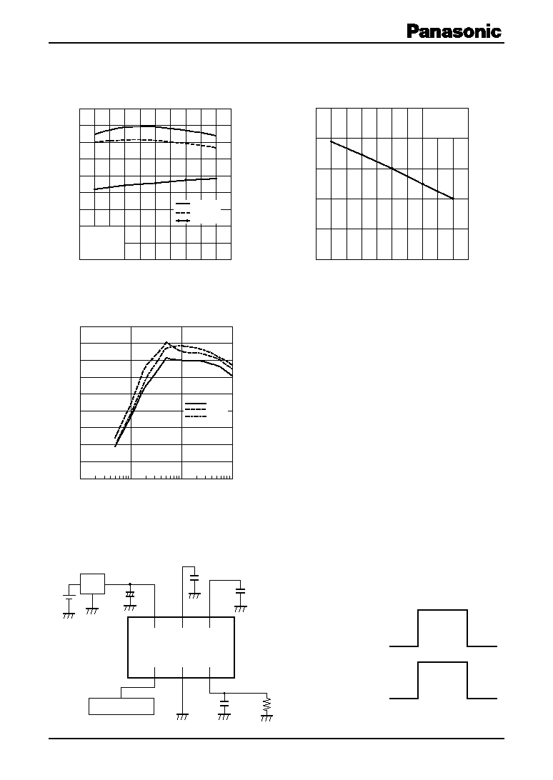
s Application Notes
1. P
D
T
a
curves of MINI-6D package
P
D
T
a
20
0
0
25
Ambient temperature T
a
(°
C)
50
75
100
125
150
40
60
80
100
120
140
Independent IC
without a heat sink
P
D
=
120 mW (25
°
C)
Po
wer dissipation P
D
(W)
Independent IC
without a heat sink
P
D
=
60 mW (75
°
C)
AN8000MS
4
SDH00013DEB
-
25
0
5
10
15
20
25
30
35
40
45
0
25
Ambient temperature
T
a
(
°
C)
V
IN
=
3.0 V
I
OUT
=
15 mA
Ripple rejection ratio RR
(dB)
50
75
f
=
25 kHz
f
=
1 kHz
f
=
100 kHz
-
25
2.6
2.62
2.64
2.66
2.68
2.7
0
25
Ambient temperature
T
a
(
°
C)
V
IN
=
3.0 V
I
OUT
=
15 mA
Output v
oltage (V)
50
75
100
1k
10k
100k
0
5
10
15
20
25
30
35
40
Ripple frequency f
rpl
(Hz)
Ripple rejection ratio RR
(dB)
65
°
C
25
°
C
-
25
°
C
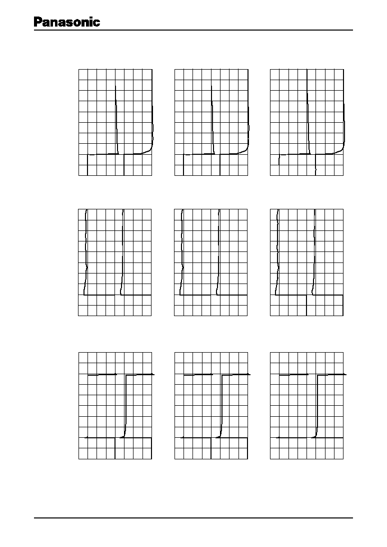
3. Transient response
1) Test circuit and conditions
6
1
5
2
4
3
AN8000MS
Reg.
SYNPWRR On
4 700 pF
0.1
µ
F
0.015
µ
F
270
0 V
3 V
3.6 V
Input
SYNPWRR On
Input
4.7
µ
F
Output
0 V
Output
V-out
s Application Notes (continued)
2. Main characteristics
RR
T
a
Output voltage
T
a
RR
f
rpl
AN8000MS
5
SDH00013DEB
2
)
Transient characteristics (SYNPWR, V
OUT
)
T
a
=
-
25
°
C
Total
Leading edge
Falling edge
T
a
=
25
°
C
T
a
=
65
°
C
0
1
2
3
0
1
2
3
(V)
2 ms/di
v
.
V
OUT
SYNPWR
0
1
2
3
0
1
2
3
(V)
2 ms/di
v
.
V
OUT
SYNPWR
0
1
2
3
0
1
2
3
(V)
2 ms/di
v
.
V
OUT
SYNPWR
0
1
2
3
0
1
2
3
10
µ
s/di
v
.
(V)
V
OUT
SYNPWR
0
1
2
3
0
1
2
3
10
µ
s/di
v
.
(V)
V
OUT
SYNPWR
0
1
2
3
0
1
2
3
10
µ
s/di
v
.
(V)
V
OUT
SYNPWR
0
1
2
3
0
1
2
3
10
µ
s/di
v
.
(V)
V
OUT
SYNPWR
0
1
2
3
0
1
2
3
10
µ
s/di
v
.
(V)
V
OUT
SYNPWR
0
1
2
3
0
1
2
3
10
µ
s/di
v
.
(V)
V
OUT
SYNPWR
s Application Notes (continued)
3. Transient response (continued)
Document Outline