1
Schottky Barrier Diodes (SBD)
MA3J700
Silicon epitaxial planar type
For high-frequency rectification
I Features
∑ S-mini type 3-pin package
∑ Allowing to rectify under (I
F(AV)
= 500 mA) condition
∑ Optimum for high-frequency rectification because of its short
reverse recovery time (t
rr
)
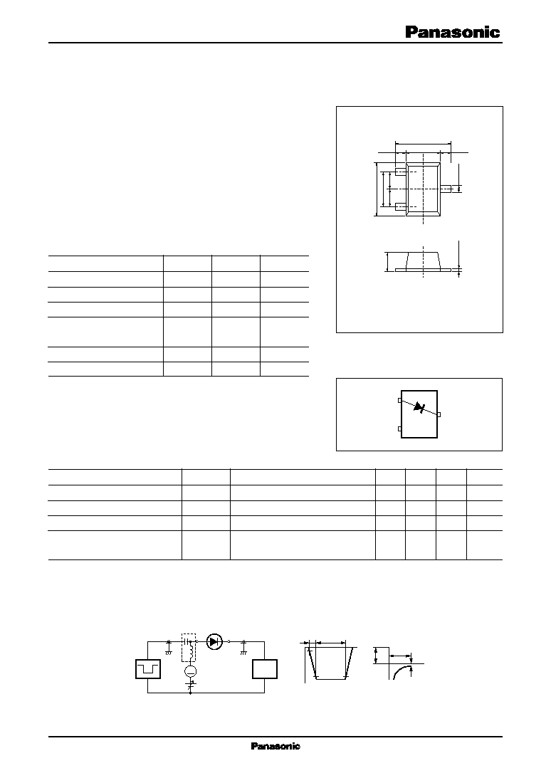
I Absolute Maximum Ratings T
a
= 25∞C
Unit : mm
Parameter
Symbol
Rating
Unit
Reverse voltage (DC)
V
R
40
V
Repetitive peak reverse voltage
V
RRM
40
V
Average forward current
I
F(AV)
500
mA
Non-repetitive peak forward
I
FSM
2
A
surge current
*
Junction temperature
T
j
125
∞C
Storage temperature
T
stg
-55 to +150
∞C
1 : Anode
2 : NC
3 : Cathode
Flat S-Mini Type Package (3-pin)
Note) * : The peak-to-peak value in one cycle of 50 Hz sine-wave
(non-repetitive)
Internal Connection
Marking Symbol: M2W
Parameter
Symbol
Conditions
Min
Typ
Max
Unit
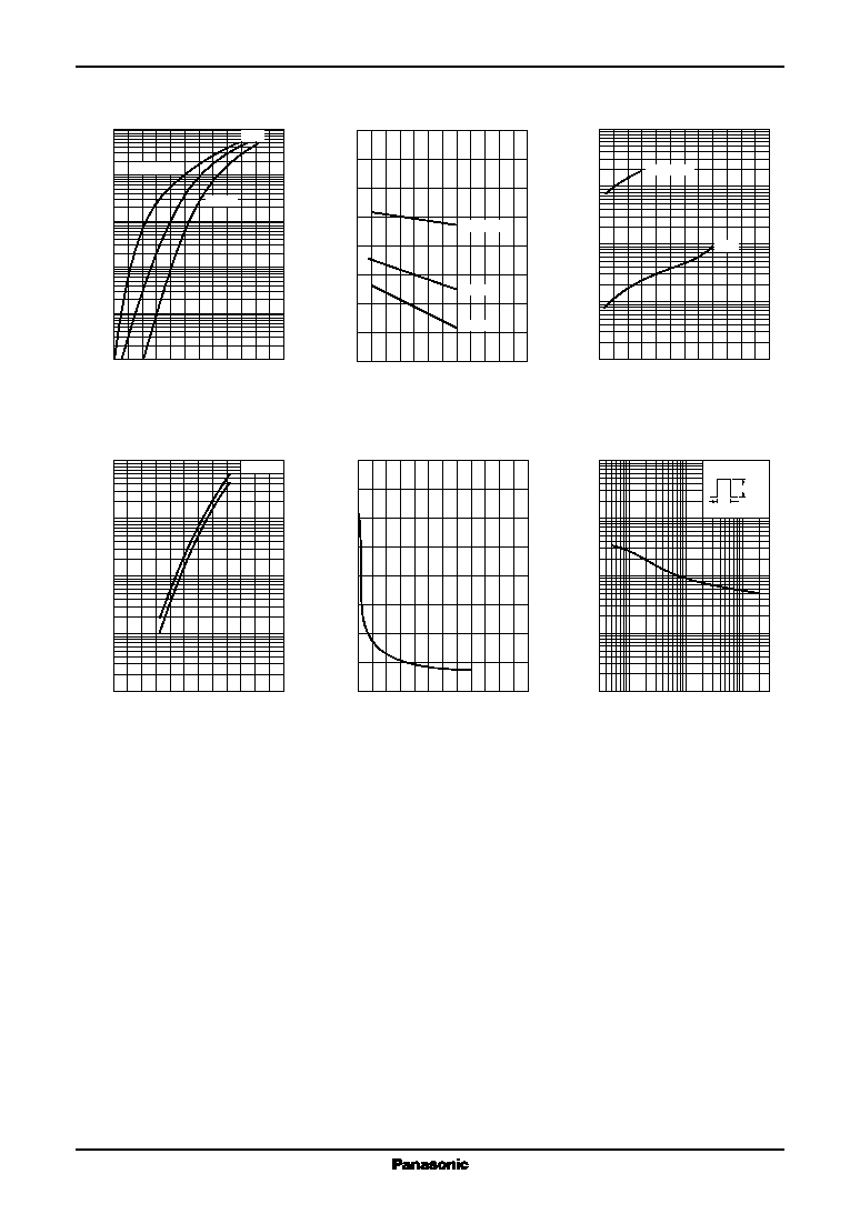
Reverse current (DC)
I
R
V
R
= 35 V
100
µA
Forward voltage (DC)
V
F
I
F
= 500 mA
0.55
V
Terminal capacitance
C
t
V
R
= 0 V, f = 1 MHz
60
pF
Reverse recovery time
*
t
rr
I
F
= I
R
= 100 mA
5
ns
I
rr
= 0.1 ∑ I
R
, R
L
= 100
I Electrical Characteristics T
a
= 25∞C
Note) 1. Schottky barrier diode is sensitive to electric shock (static electricity, etc.). Due attention must be paid on the charge of a
human body and the leakage of current from the operating equipment.
2. Rated input/output frequency: 400 MHz
3. * : t
rr
measuring circuit
1
2
3
1.25
± 0.1
1.3
±
0.1
2.0
±
0.2
0.9
±
0.1
0.65
0.65
0.425
0.425
0.3
+
0.1
-
0
2.1
± 0.1
0.15
+
0.1
-
0.05
1
2
3
Bias Application Unit N-50BU
90%
Pulse Generator
(PG-10N)
R
s
= 50
W.F.Analyzer
(SAS-8130)
R
i
= 50
t
p
= 2 µs
t
r
= 0.35 ns
= 0.05
I
F
= 100 mA
I
R
= 100 mA
R
L
= 100
10%
Input Pulse
Output Pulse
I
rr
= 0.1 ∑ I
R
t
r
t
p
t
rr
V
R
I
F
t
t
A