For Video Equipment
MN3111H
Vertical Driver LSI for Video Camera CCD Area Image Sensor
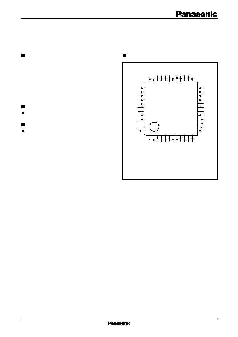
Pin Assignment
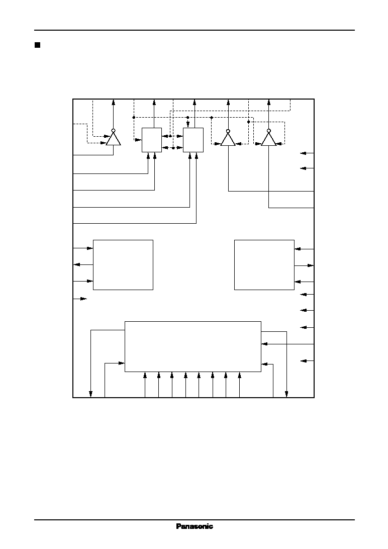
Overview
The MN3111H is a vertical driver LSI for a two-dimen-
sional interline CCD image sensor. It features a built-in
power supply circuit that, in conjunction with such
external components as four booster capacitors, six volt-
age stabilization capacitors, eight Schottky barrier diodes,
and two Zener diodes, produces stabilized +15.0V and
≠10.0V power supplies from a +5.0V input and HD pulses.
Features
Single 5 volt power supply
Applications
Video cameras
QFH048-P-0707
(TOP VIEW)
OV
EE
C3+
GND
C2≠
C3 ≠
C2+
C1+
C1≠
V
CC1
C4+
OV
DD
HD
V
EE
V
HH
OSUB
V
L2
V
L1
OV1
V
M13
OV3
OV2
V
M24
OV4
V
H
V
DD
V
CC2
IV2
IV4
SENSE1
V
OUT+
N.C.
V
IN+
CAP3
CAP2
CAP1
TEST
ISUB
CH1
IV1
IV3
CH2
SENSE2
V
OUT≠
V
IN ≠
GND
N.C.
N.C.
C4 ≠
1
2
3
4
5
6
7
8
9
10
11
12
24
23
22
21
20
19
18
17
16
15
14
13
37
38
39
40
41
42
43
44
45
46
47
48
36
35
34
33
32
31
30
29
28
27
26
25
For Video Equipment
MN3111H
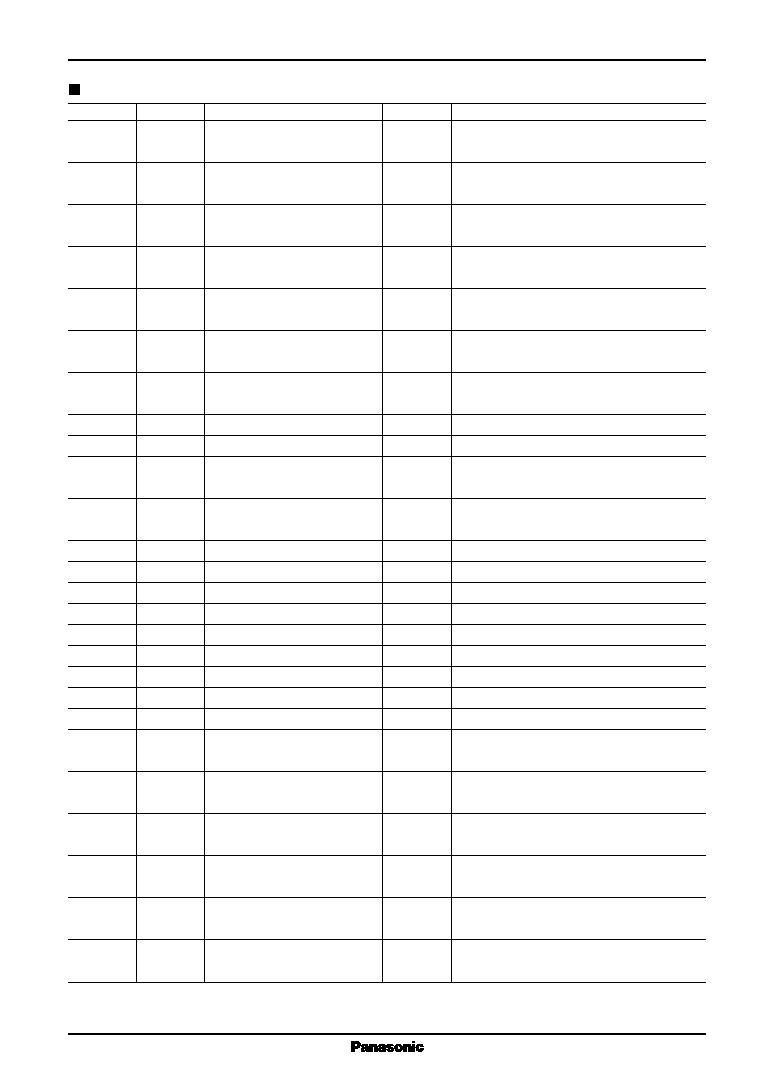
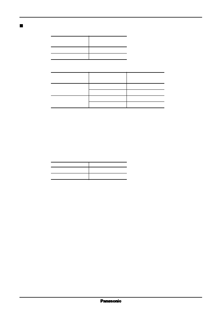
Pin Descriptions
Pin No.
Symbol
Pin Name
I/O
Function Description
9
V
CC1
"H" level power supply
I
"H" level input for 5 volt circuits
23
V
CC2
for input block
3
GND
"L" level power supply
I
"L" level input for 5 volt circuits
45
for input block
25
V
H
"H" level power supply
I
"H" level input for high-voltage circuits
for vertical driver
35
V
HH
"H" level power supply
I
"H" level input for high-voltage circuits
for SUB driver
30
V
M13
"M" level power supply
I
"M" level input for high-voltage circuits
27
V
M24
for vertical driver
32
V
L1
"L" level power supply
I
"L" level input for high-voltage circuits
for vertical driver
33
V
L2
"L" level power supply
I
"L" level input for high-voltage circuits
for SUB driver
24
V
DD
Driver power supply 1
I
"H" level for high-voltage circuits
36
V
EE
Driver power supply 2
I
"L" level for high-voltage circuits
17
V
IN+
Voltage input for positive
I
Voltage input pin for positive voltage
voltage monitor
monitor
44
V
IN ≠
Voltage input for negative
I
Voltage input pin for negative voltage
voltage monitor
monitor
13
TEST
Test input
I
Test pin (Keep this pin at "H" level.)
12
HD
HD pulse input
I
HD pulse input pin
22
IV2
Transfer pulse input
I
Charge transfer pulse input pin
21
IV4
Transfer pulse input
I
Charge transfer pulse input pin
39
IV1
Transfer pulse input
I
Charge transfer pulse input pin
40
IV3
Transfer pulse input
I
Charge transfer pulse input pin
38
CH1
Charge pulse input
I
Charge readout pulse input pin
41
CH2
Charge pulse input
I
Charge readout pulse input pin
37
ISUB
SUB pulse input
I
Unwanted charge rejection pulse input pin
20
SENSE1
Positive voltage monitor
I
Positive voltage monitor control sensing
sensing input
pin (Leave this pin open.)
42
SENSE2
Negative voltage monitor
I
Negative voltage monitor control sensing
sensing input
pin (Leave this pin open.)
7
C1+
C1 connection
O
Booster block voltage charging capacitor
8
C1≠
connection pins
6
C2+
C2 connection
O
Booster block voltage charging capacitor
4
C2≠
connection pins
2
C3+
C3 connection
O
Booster block voltage charging capacitor
5
C3 ≠
connection pins
10
C4+
C4 connection
O
Booster block voltage charging capacitor
48
C4 ≠
connection pins
MN3111H
For Video Equipment
Pin Descriptions (continued)
Pin No.
Symbol
Pin Name
I/O
Function Description
11
OV
DD
Booster block positive
O
Booster block positive voltage
voltage output
output pin
1
OV
EE
Booster block negative
O
Booster block negative voltage
voltage output
output pin
19
V
OUT+
Positive regulated voltage
O
Positive voltage monitor output pin
output
(Leave this pin open.)
43
V
OUT-
Negative regulated voltage
O
Negative voltage monitor output pin
output
(Leave this pin open.)
26
OV4
Binary transfer pulse
O
Binary (V
M24
, V
L1
) transfer pulse
output
output pin
28
OV2
Binary transfer pulse
O
Binary (V
M24
, V
L1
) transfer pulse
output
output pin
29
OV3
Tristate transfer pulse
O
Tristate (V
H
, V
M13
, V
L1
) transfer pulse
output
output pin
31
OV1
Tristate transfer pulse
O
Tristate (V
H
, V
M13
, V
L1
) transfer pulse
output
output pin
34
OSUB
SUB pulse output
O
Unwanted charge (V
HH
, V
L2
) rejection
pulse input pin
14
CAP1
Stabilizing capacitor
O
Pins for connecting capacitors for internal
15
CAP2
connection
voltage stabilization circuits
16
CAP3
18
N.C.
No connection
--
46
47
For Video Equipment
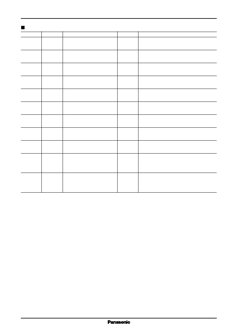
MN3111H
Functional Description
Binary transfer pulses (vertical driver block)
IV2
OV2
IV4
OV4
H
L
L
M
Tristate transfer pulses (vertical driver block)
CH1
IV1
OV1
CH2
IV3
OV3
H
H
L
L
M
L
H
L
L
H
*1 IV1, IV2, IV3, IV4, CH1, CH2
H: V
CC
L: GND
OV1, OV2, OV3, OV4
H: V
H
M: V
M13
, or V
M24
L: V
L1
Unwanted charge rejection pulses (SUB driver block)
ISUB
OSUB
H
L
L
H
*1 ISUB
H: V
CC
L: GND
OSUB
H: V
HH
L: V
L2