Switching Diodes
1
MA6X121
Silicon epitaxial planar type
I Features
∑ Three-element contained in one package, allowing high-density
mounting
∑ Short reverse recovery time t
rr
∑ Small terminal capacitance, C
t
I Absolute Maximum Ratings T
a
= 25∞C
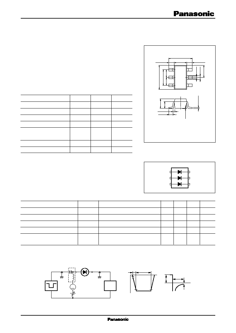
Unit : mm
Parameter
Symbol
Rating
Unit
Reverse voltage (DC)
V
R
80
V
Peak reverse voltage
V
RM
80
V
Forward current (DC)
*1
I
F
100
mA
Peak forward current
*1
I
FM
225
mA
Non-repetitive peak forward
I
FSM
500
mA
surge current
*1,2
Junction temperature
T
j
150
∞C
Storage temperature
T
stg
-55 to +150
∞C
Parameter
Symbol
Conditions
Min
Typ
Max
Unit
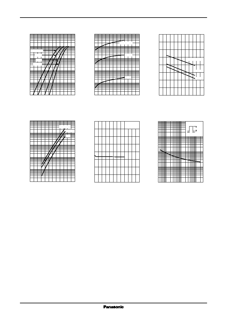
Reverse current (DC)
I
R
V
R
= 75 V
100
nA
Forward voltage (DC)
V
F
I
F
= 100 mA
1.2
V
Reverse voltage (DC)
V
R
I
R
= 100 µA
80
V
Terminal capacitance
C
t
V
R
= 0 V, f = 1 MHz
2
pF
Reverse recovery time
*
t
rr
I
F
= 10 mA, V
R
= 6 V
3
ns
I
rr
= 0.1 ∑ I
R
, R
L
= 100
I Electrical Characteristics T
a
= 25∞C
Note) 1. Rated input/output frequency: 100 MHz
2. * : t
rr
measuring circuit
Marking Symbol: M2D
2.8
+ 0.2
- 0.3
1.5
+ 0.25
- 0.05
0.65
± 0.15
0.65
± 0.15
1
6
5
4
3
2
1.45
±
0.1
0.95
0.95
1.9
±
0.2
0.3
+
0.1
-
0.05
0.5
+
0.1
-
0.05
2.9
+
0.2
-
0.05
1.1
+
0.2
-
0.1
0.8
0.4
± 0.2
0 to 0.1
0.16
+
0.1
-
0.06
0.1 to 0.3
Note) *1 : Value for single diode
*2 : t = 1 s
1 : Cathode 1
4 : Anode 3
2 : Cathode 2
5 : Anode 2
3 : Cathode 3
6 : Anode 1
Mini Type Package (6-pin)
Internal Connection
6
5
4
1
2
3
Bias Application Unit N-50BU
90%
Pulse Generator
(PG-10N)
R
s
= 50
W.F.Analyzer
(SAS-8130)
R
i
= 50
t
p
= 2 µs
t
r
= 0.35 ns
= 0.05
I
F
= 10 mA
V
R
= 6 V
R
L
= 100
10%
Input Pulse
Output Pulse
I
rr
= 0.1 ∑ I
R
t
r
t
p
t
rr
V
R
I
F
t
t
A