 | –≠–ª–µ–∫—Ç—Ä–æ–Ω–Ω—ã–π –∫–æ–º–ø–æ–Ω–µ–Ω—Ç: ON3732A | –°–∫–∞—á–∞—Ç—å:  PDF PDF  ZIP ZIP |
1
Optoisolators (Photocouplers)
CNZ3731, CNC7C501, CNZ3734
CNC2S501, CNC7C502, CNC7H501
Optoisolators
Overview
The CNZ3731 series of optoisolators consist of a GaAs infrared
LED which is optically coupled with a Si NPN Darlington
phototransistor, and housed in a small DIL package. The series
provides high I/O isolation voltage and high collector/emitter isolation
voltage, as well as a high current transfer ratio (CTR). This opto
isolator series also includes the two-channel CNC7C501 and the four-
channel CNZ3734, and A type of these models with increased
collector to emitter breakdown voltage (V
CEO
> 350V).
Features
High collector to emitter breakdown voltage : V
CEO
> 300 V,
A type : V
CEO
> 350 V
High current transfer ratio with Darlington phototransistor output :
CTR = 4000% (typ.)
High I/O isolation voltage : V
ISO
5000 V
rms
Small DIL package for saving mounting space
UL listed (UL File No. E79920)
A-type models have a guaranteed internal insulating distance of 0.4 mm
Applications
Telephones
Telephone exchange
FAX
Programmable controllers
Signal transfer between circuits with different potentials and impedances
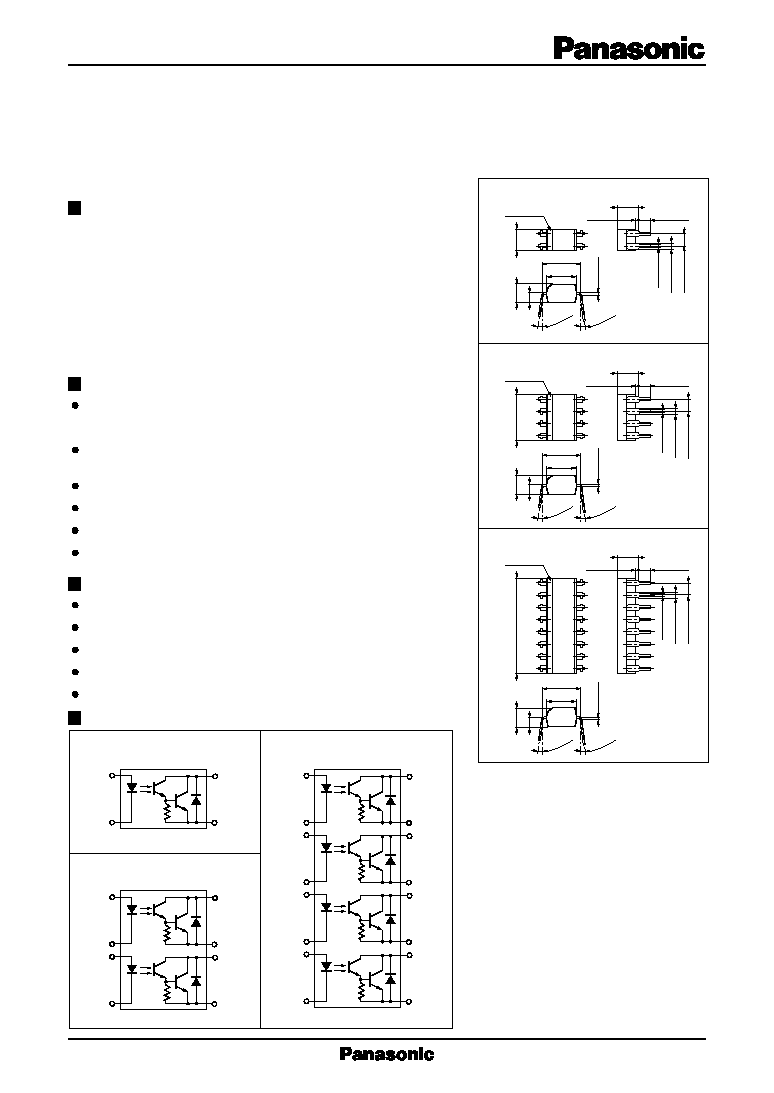
Unit : mm
CNZ3731/CNC2S501
CNC7C501/CNC7C502
CNZ3734/CNC7H501
Unit : mm
Unit : mm
1 , 3 , 5 , 7 :
2 , 4 , 6 , 8 :
9,11,13,15:
10,12,14,16:
1: Anode
2: Cathode
3: Emitter
4: Collector
1,3: Anodee
2,4: Cathode
5,7: Emitter
6,8: Collector
Anode
Cathode
Emitter
Collector
0 to 15∞
0 to 15∞
0 to 15∞
0 to 15∞
1
2
3
4
4.58
±
0.3
1
2
3
4
7
8
5
6
9.66
±
0.3
0.25
4-0.5
±
0.1
4-1.2
±
0.15
2.54
±
0.25
2.0
3.85
±
0.3
+0.15 ≠0
7.62
±
0.3
2.54 min.
0.5 min.
6.2
±
0.5
0.25
2.0
3.85
±
0.3
+0.15 ≠0
7.62
±
0.3
6.2
±
0.5
1
2
3
4
5
6
7
8
13
14
15
16
9
10
11
12
19.82
±
0.5
0 to 15∞
0 to 15∞
0.25
2.0
3.85
±
0.3
+0.15 ≠0
7.62
±
0.3
6.2
±
0.5
5.2 max.
8-0.5
±
0.1
8-1.2
±
0.15
2.54
±
0.25
2.54 min.
0.5 min.
5.2 max.
16-0.5
±
0.1
16-1.2
±
0.15
2.54
±
0.25
2.54 min.
0.5 min.
5.2 max.
LED Mark
LED Mark
LED Mark
Pin Connection
Top View
CNZ3731
CNC2S501
Top View
CNC7C501
CNC7C502
1
2
4
3
1
2
8
7
3
4
6
5
1
2
16
15
3
4
14
13
5
6
12
11
7
8
10
9
CNZ3734
CNC7H501
Top View

2
CNZ3731, CNC7C501, CNZ3734, CNC2S501, CNC7C502, CNC7H501
Optoisolators (Photocouplers)
Absolute Maximum Ratings
(Ta = 25∞C)
Parameter
Symbol
Ratings
Unit
CNZ3731
CNC2S501
Reverse voltage (DC)
V
R
6
6
V
Input (Light
Forward current (DC)
I
F
50
50
mA
emitting diode)
Pulse forward current
I
FP
*1
1
1
A
Power dissipation
P
D
*2
75
75
mW
Collector current
I
C
150
150
mA
Output (Photo Collector to emitter voltage
V
CEO
300
350
V
transistor)
Emitter to collector voltage
V
ECO
0.3
0.3
V
Collector power dissipation
P
C
*3
300
150
300
150
mW
Total power dissipation
P
T
320
200
320
200
mW
Isolation voltage, input to output
V
ISO
*4
5000
5000
V
rms
Operating ambient temperature
T
opr
≠30 to +100
≠30 to +100
∞C
Storage temperature
T
stg
≠55 to +125
≠55 to +125
∞C
*1
Pulse width
100
µ
s, repeat 100 pps
*2
Input power derating ratio is 0.75 mW/∞C at Ta
25∞C.
*3
Output power derating ratio is 3.0 mW/∞C at Ta
25∞C (CNZ3731, CNC2S501).
Output power derating ratio is 0.75 mW/∞C at Ta
25∞C (CNC7C501, CNC2S502, CNZ3734, CNC7H501).
*4
AC 1min., RH < 60 %
CNC7C502
CNC7H501
CNC7C501
CNZ3734
Electrical Characteristics
(Ta = 25∞C)
Parameter
Symbol
Conditions
min
typ
max
Unit
Input
Reverse current (DC)
I
R
V
R
= 3V
10
µ
A
characteristics
Forward voltage (DC)
V
F
I
F
= 50mA
1.35
1.5
V
Capacitance between pins
C
t
V
R
= 0V, f
= 1MHz
30
pF
Output
Collector cutoff current
I
CEO
V
CE
= 200V
200
nA
characteristics Collector to emitter capacitance
C
C
V
CE
= 10V, f
= 1MHz
10
pF
DC current transfer ratio
CTR
*1
V
CE
= 2V, I
F
= 1mA
1000
4000
%
Isolation capacitance, input to output
C
ISO
f
= 1MHz
0.7
pF
Transfer
Isolation resistance, input to output
R
ISO
V
ISO
= 500V
10
11
characteristics Rise time
t
r
*2
V
CC
= 10V, I
C
= 10mA,
40
µ
s
Fall time
t
f
*3
R
t
= 100
15
µ
s
Collector to emitter saturation voltage V
CE(sat)
I
F
= 1mA, I
C
= 2mA
1.0
V
*1
DC current transfer ratio (CTR) is a ratio of output current against DC input current.
I
C
CTR =
◊
100 (%)
I
F
*2
t
r
: Time required for the collector current to increase from 10% to 90% of its final value
*3
t
f
: Time required for the collector current to decrease from 90% to 10% of its initial value
3
Optoisolators (Photocouplers)
CNZ3731, CNC7C501, CNZ3734, CNC2S501, CNC7C502, CNC7H501
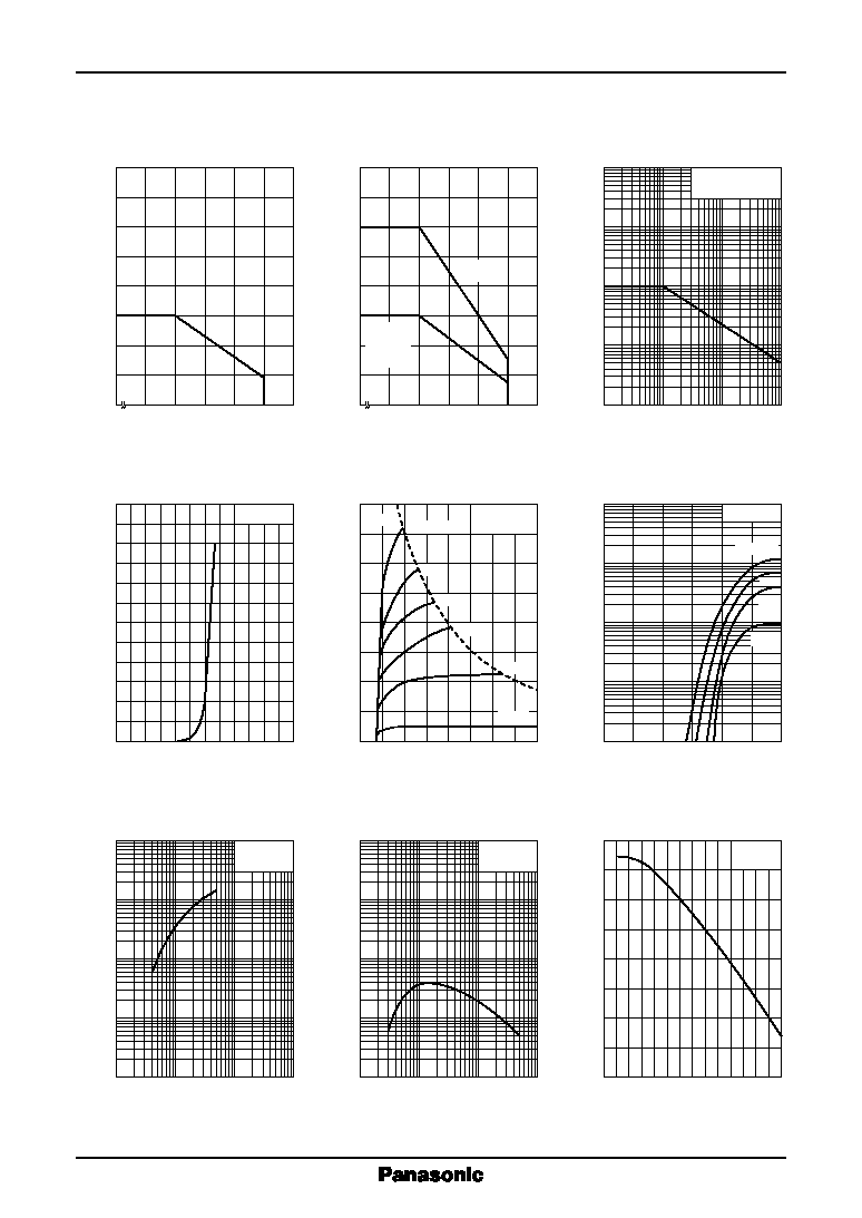
I
F
-- V
F
60
30
20
10
50
40
Forward voltage V
F
(V)
Forward current I
F
(mA)
0.4
0.8
1.2
1.6
2.4
2.0
0
0
Ta = 25∞C
P
D
-- Ta
200
150
100
50
Ambient temperature Ta (∞C )
LED Power dissipation P
D
(mW)
25
75
125
0
50
100
0
≠ 30
I
FP
-- D
R
10
5
10
4
10
3
10
2
Duty ratio D
R
Allowable pulse forward current I
FP
(mA)
1
10
Pulse width
100
µ
s
Ta = 25∞C
10
≠1
10
≠2
10
≠3
Relative CTR -- Ta
120
100
80
60
Ambient temperature Ta (∞C )
Relative DC current transfer ratio CTR (%)
40
I
F
= 1mA
V
CE
= 2V
I
C
-- I
F
10
3
10
2
10
1
Forward current I
F
(mA)
Collector current I
C
(mA)
1
10
10
2
10
≠1
10
≠1
V
CE
= 2V
Ta = 25∞C
CTR -- I
F
10
6
10
3
10
5
10
4
Forward current I
F
(mA)
DC current transfer ratio CTR (%)
1
10
10
2
10
2
10
≠1
V
CE
= 2V
Ta = 25∞C
I
C
-- V
CE
160
40
80
120
Collector to emitter voltage V
CE
(V)
Collector current I
C
(mA)
2
4
8
6
0
0
Ta = 25∞C
P
C
-- Ta
400
300
200
100
Ambient temperature Ta (∞C )
Collector power dissipation P
C
(mW)
25
75
125
0
50
100
0
≠ 30
I
C
-- V
CE(sat)
Collector saturation voltage V
CE(sat)
(V)
Collector current I
C
(mA)
10
3
10
2
10
1
10
≠1
Ta = 25∞C
0
0.4
0.8
1.2
0
20
40
60
80
100
≠ 40 ≠ 20
CNZ3731
CNC2S501
CNC7C501/
CNC7C502
CNZ3734/
CNC7H501
I
F
= 5mA
3mA
2mA
1.5mA
Pc(max.)
0.5mA
1mA
0.5mA
2mA
1mA
I
F
= 5mA

4
CNZ3731, CNC7C501, CNZ3734, CNC2S501, CNC7C502, CNC7H501
Optoisolators (Photocouplers)
≠ 40 ≠ 20
0
40
80
20
60
100
I
CEO
-- Ta
10
≠5
10
≠9
10
≠10
10
≠7
10
≠8
10
≠6
Ambient temperature Ta (∞C )
V
CE
= 200V
Dark current I
CEO
(A)
10
≠11
10
10
≠3
10
≠2
I
CEO
-- V
CE
10
≠9
10
≠8
Collector to emitter voltage V
CE
(V)
Ta = 25∞C
Dark current I
CEO
(A)
10
≠10
V
CE(sat)
-- Ta
1.6
1.4
1.2
1.0
0.8
Ambient temperature Ta (∞C )
Collector to emitter saturation voltage V
CE(sat)
(V)
0
20
40
60
80
100
0.4
0.6
≠ 40 ≠ 20
I
F
= 1mA
I
C
= 2mA
Response time --
External load resistance characteristics
10
3
10
2
10
1
External load resistance R
L
(k
)
Response time (
µ
s)
10
≠1
1
10
10
≠1
10
≠2
V
CC
= 10V
I
C
= 10mA
Ta = 25∞C
Frequency characteristics
Response time measurement circuit
Measurement circuit of
frequency characteristics
Frequency f (kHz)
Voltage gain A
V
(dB)
10
0
≠ 10
≠ 20
10
1
10
2
10
3
≠ 30
10
≠1
V
CE
= 4V
Ta = 25∞C
I
C
= 10mA
t
r
t
f
t
d
t
s
R
L
=
10
1k
100
,,
,
,,
,,
50
5k
50
50k
V
CC
R
L
,,
,,
,,,
,
50
Sig.IN
R
L
V
CC
10%
90%
t
d
t
r
t
f
t
s
,
,
+10V
16V
100
µ
F
Sig.OUT
Sig.IN
≠
+
I
C
= 10mA
4mAp - p
5ms
V
1
V
1
V
2