 | –≠–ª–µ–∫—Ç—Ä–æ–Ω–Ω—ã–π –∫–æ–º–ø–æ–Ω–µ–Ω—Ç: UNR4113 | –°–∫–∞—á–∞—Ç—å:  PDF PDF  ZIP ZIP |
Transistors with built-in Resistor
1
Publication date: December 2003
SJH00018DED
UNR411x Series
(UN411x Series)
Silicon PNP epitaxial planar type
For digital circuits
Features
∑ Costs can be reduced through downsizing of the equipment and
reduction of the number of parts
∑ New S type package, allowing supply with the radial taping
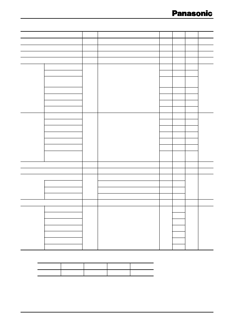
Resistance by Part Number
(R
1
)
(R
2
)
∑ UNR4110 (UN4110)
47 k
∑ UNR4111 (UN4111)
10 k
10 k
∑ UNR4112 (UN4112)
22 k
22 k
∑ UNR4113 (UN4113)
47 k
47 k
∑ UNR4114 (UN4114)
10 k
47 k
∑ UNR4115 (UN4115)
10 k
∑ UNR4116 (UN4116)
4.7 k
∑ UNR4117 (UN4117)
22 k
∑ UNR4118 (UN4118)
0.51 k
5.1 k
∑ UNR4119 (UN4119)
1 k
10 k
∑ UNR411D (UN411D)
47 k
10 k
∑ UNR411E (UN411E)
47 k
22 k
∑ UNR411F (UN411F)
4.7 k
10 k
∑ UNR411H (UN411H)
2.2 k
10 k
∑ UNR411L (UN411L)
4.7 k
4.7 k
∑ UNR411M
2.2 k
47 k
∑ UNR411N
4.7 k
47 k
Absolute Maximum Ratings T
a
= 25∞C
B
R
1
R
2
C
E
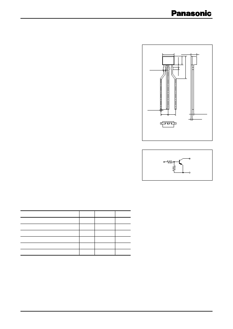
Internal Connection
Unit: mm
1: Emitter
2: Collector
3: Base
NS-B1 Package
Note) The part numbers in the parenthesis show conventional part number.
Parameter
Symbol
Rating
Unit
Collector-base voltage (Emitter open)
V
CBO
-50
V
Collector-emitter voltage (Base open)
V
CEO
-50
V
Collector current
I
C
-100
mA
Total power dissipation
P
T
300
mW
Junction temperature
T
j
150
∞C
Storage temperature
T
stg
-55 to +150
∞C
4.0
±0.2
0.75 max.
2.0
±0.2
0.45
(2.5) (2.5)
0.7
±0.1
2
3
1
+0.20
≠0.10
0.45
+0.20
≠0.10
7.6
3.0
±
0.2
(0.8)
(0.8)
15.6
±
0.5
2
UNR411x Series
SJH00018DED
Electrical Characteristics T
a
= 25∞C ± 3∞C
Parameter
Symbol
Conditions
Min
Typ
Max
Unit
Collector-base voltage (Emitter open)
V
CBO
I
C
= -10 µA, I
E
= 0
-50
V
Collector-emitter voltage (Base open)
V
CEO
I
C
= -2 mA, I
B
= 0
-50
V
Collector-base cutoff current (Emitter open)
I
CBO
V
CB
= -50 V, I
E
= 0
- 0.1
µA
Collector-emitter cutoff current (Base open)
I
CEO
V
CE
= -50 V, I
B
= 0
- 0.5
µA
Emitter-base
UNR4110/4115/4116/4117
I
EBO
V
EB
= -6 V, I
C
= 0
- 0.01
mA
cutoff current UNR4113
- 0.1
(Collector open) UNR4112/4114/411D/
- 0.2
411E/411M/411N
UNR4111
- 0.5
UNR411F/411H
-1.0
UNR4119
-1.5
UNR4118/411L
-2.0
Forward current UNR4118/411L
h
FE
V
CE
= -10 V, I
C
= -5 mA
20
transfer ratio
UNR4119/411D/411F/411H
30
UNR4111
35
UNR4112/411E
60
UNR4113/4114/411M
80
UNR411N
80
400
UNR4110
*
/4115
*
/4116
*
/
160
460
4117
*
Collector-emitter saturation voltage
V
CE(sat)
I
C
= -10 mA, I
B
= - 0.3 mA
- 0.25
V
Output voltage high-level
V
OH
V
CC
= -5 V, V
B
= - 0.5 V, R
L
= 1 k
-4.9
V
Output voltage low-level
V
OL
V
CC
= -5 V, V
B
= -2.5 V, R
L
= 1 k
- 0.2
V
UNR4113
V
CC
= -5 V, V
B
= -3.5 V, R
L
= 1 k
UNR411D
V
CC
= -5 V, V
B
= -10 V, R
L
= 1 k
UNR411E
V
CC
= -5 V, V
B
= -6 V, R
L
= 1 k
Transition frequency
f
T
V
CB
= -10 V, I
E
= 1 mA, f = 200 MHz
80
MHz
Input resistance UNR4118
R
1
-30%
0.51
+30%
k
UNR4119
1.0
UNR411H/411M
2.2
UNR4116/411F/411L/411N
4.7
UNR4111/4114/4115
10
UNR4112/4117
22
UNR4110/4113/411D/411E
47
Note) 1. Measuring methods are based on JAPANESE INDUSTRIAL STANDARD JIS C 7030 measuring methods for transistors.
2. *: Rank classification
Rank
Q
R
S
No-rank
h
FE
160 to 260
210 to 340
290 to 460
160 to 460
3
UNR411x Series
SJH00018DED
I
C
V
CE
V
CE(sat)
I
C
h
FE
I
C
P
T
T
a
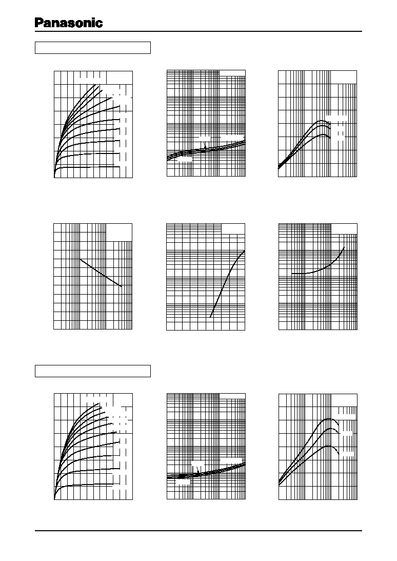
Common characteristics chart
Characteristics charts of UNR4110
0
0
-12
-2
-10
-4
-8
-6
-120
-100
-80
-60
-40
-20
Collector-emitter voltage V
CE
(V)
Collector current I
C
(mA
)
T
a
= 25∞C
I
B
= -1.0 mA
- 0.9 mA
- 0.8 mA
- 0.7 mA
- 0.6 mA
- 0.5 mA
- 0.4 mA
- 0.3 mA
- 0.2 mA
- 0.1 mA
- 0.01
-0.1
- 0.1
-1
-10
-100
-1
-10
-100
Collector-emitter saturation voltage V
CE(sat)
(V
)
Collector current I
C
(mA)
I
C
/ I
B
= 10
T
a
= 75∞C
25
∞C
-25∞C
0
-1
100
200
300
400
-10
-100
-1 000
Forward current transfer ratio h
FE
Collector current I
C
(mA)
V
CE
= ≠10 V
T
a
= 75∞C
25
∞C
-25∞C
0
0
160
40
120
80
100
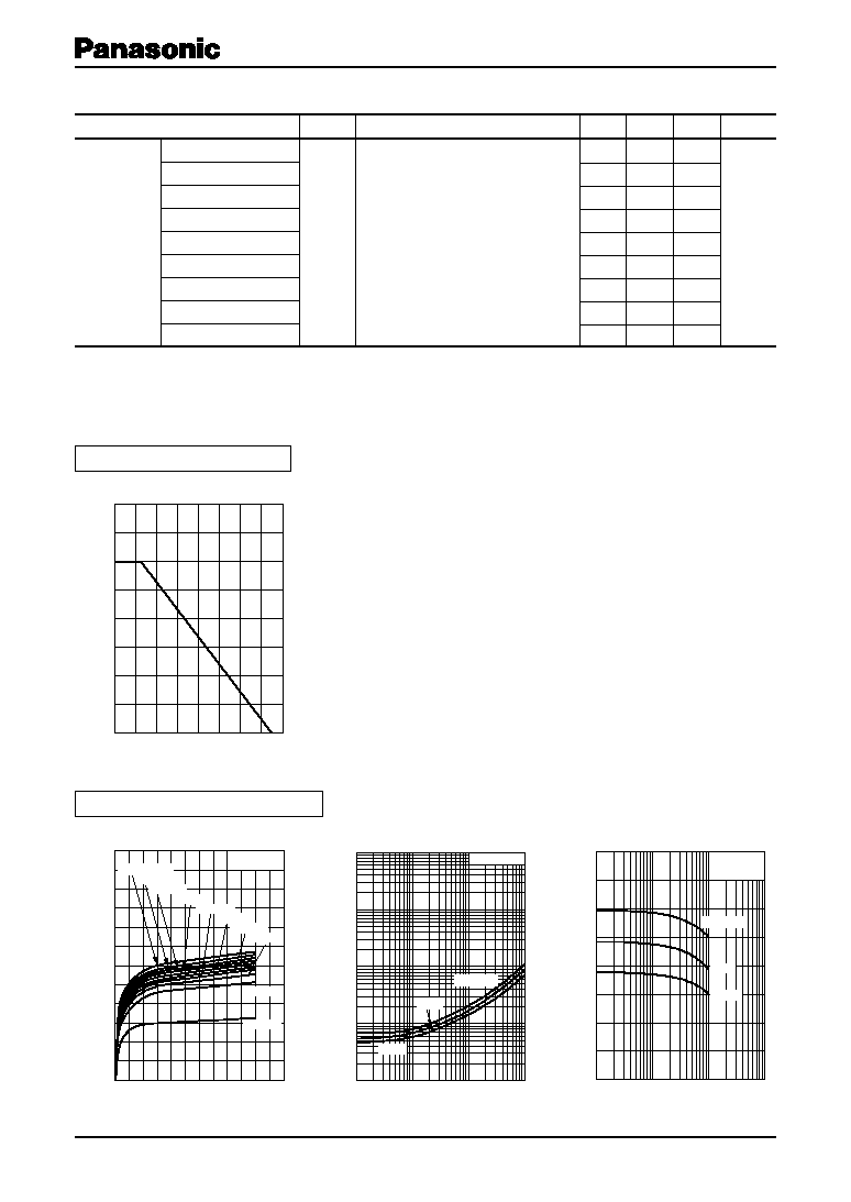
300
200
400
Ambient temperature T
a
(
∞C)
Total power dissipation P
T
(mW)
Electrical Characteristics (continued) T
a
= 25∞C ± 3∞C
Parameter
Symbol
Conditions
Min
Typ
Max
Unit
Resistance ratio UNR411M
R
1
/R
2
0.047
UNR411N
0.1
UNR4118/4119
0.08
0.10
0.12
UNR4114
0.17
0.21
0.25
UNR411H
0.17
0.22
0.27
UNR411F
0.37
0.47
0.57
UNR4111/4112/4113/411L
0.8
1.0
1.2
UNR411E
1.70
2.14
2.60
UNR411D
3.7
4.7
5.7
Note) Measuring methods are based on JAPANESE INDUSTRIAL STANDARD JIS C 7030 measuring methods for transistors.
4
UNR411x Series
SJH00018DED
C
ob
V
CB
I
O
V
IN
V
IN
I
O
I
C
V
CE
V
CE(sat)
I
C
h
FE
I
C
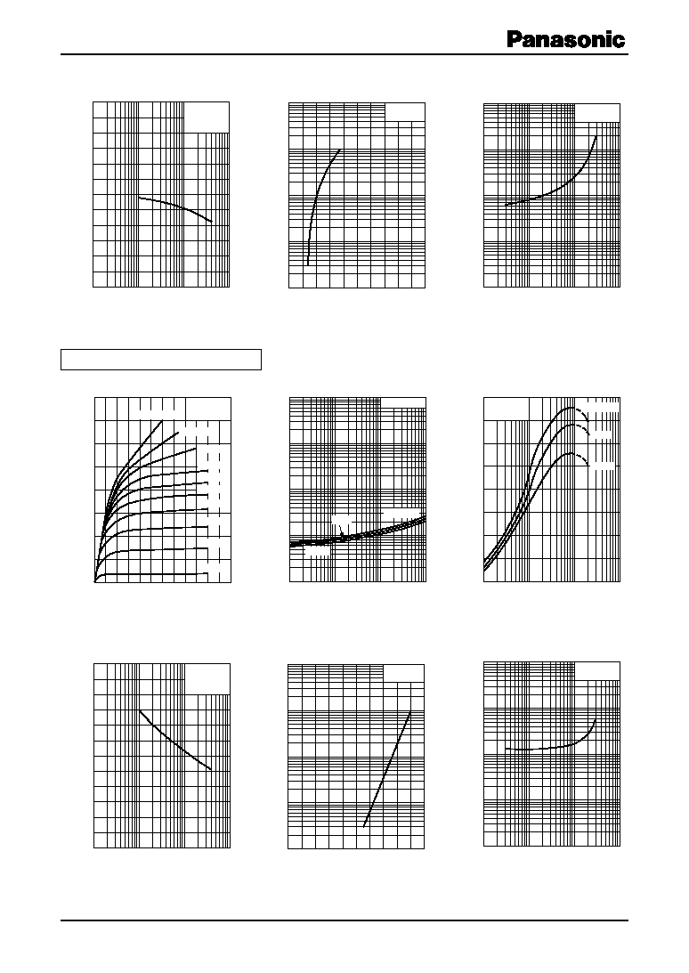
Characteristics charts of UNR4111
C
ob
V
CB
I
O
V
IN
V
IN
I
O
0
- 0.1
6
5
4
3
2
1
-1
-10
-100
Collector output capacitance
(Common base, input open circuited)
C
ob
(pF)
Collector-base voltage V
CB
(V)
f
= 1 MHz
I
E
= 0
T
a
= 25∞C
-1
- 0.4
-10
-10
2
-10
3
-10
4
-1.4
-1.2
-1.0
- 0.8
- 0.6
Output current I
O
(µ
A
)
Input voltage V
IN
(V)
V
O
= -5 V
T
a
= 25∞C
- 0.01
- 0.1
- 0.1
-1
-10
-100
-1
-10
-100
Input voltage V
IN
(V
)
Output current I
O
(mA)
V
O
= - 0.2 V
T
a
= 25
∞C
0
0
-12
-2
-10
-4
-8
-6
-40
-120
-80
-160
Collector-emitter voltage V
CE
(V)
Collector current I
C
(mA
)
T
a
= 25∞C
I
B
= -1.0 mA
- 0.9 mA
- 0.8 mA
- 0.7 mA
- 0.6 mA
- 0.5 mA
- 0.4 mA
- 0.3 mA
- 0.2 mA
- 0.1 mA
- 0.01
- 0.1
- 0.1
-1
-10
-100
-1
-10
-100
Collector-emitter saturation voltage V
CE(sat)
(V
)
Collector current I
C
(mA)
I
C
/ I
B
= 10
T
a
= 75∞C
25
∞C
-25∞C
0
-1
40
80
120
160
-10
-100
-1 000
Forward current transfer ratio h
FE
Collector current I
C
(mA)
V
CE
= -10 V
T
a
= 75∞C
25
∞C
-25∞C
-1
- 0.4
-10
-10
2
-10
3
-10
4
-1.4
-1.2
-1.0
- 0.8
- 0.6
Output current I
O
(µ
A
)
Input voltage V
IN
(V)
V
O
= -5 V
T
a
= 25∞C
0
- 0.1
6
5
4
3
2
1
-1
-10
-100
Collector output capacitance
(Common base, input open circuited)
C
ob
(pF)
Collector-base voltage V
CB
(V)
f
= 1 MHz
I
E
= 0
T
a
= 25∞C
- 0.01
- 0.1
- 0.1
-1
-10
-100
-1
-10
-100
Input voltage V
IN
(V
)
Output current I
O
(mA)
V
O
= - 0.2 V
T
a
= 25∞C
5
UNR411x Series
SJH00018DED
I
C
V
CE
V
CE(sat)
I
C
h
FE
I
C
C
ob
V
CB
I
O
V
IN
V
IN
I
O
Characteristics charts of UNR4112
I
C
V
CE
V
CE(sat)
I
C
h
FE
I
C
Characteristics charts of UNR4113
0
0
-12
-2
-10
-4
-8
-6
-40
-120
-80
-160
Collector-emitter voltage V
CE
(V)
Collector current I
C
(mA
)
T
a
= 25∞C
I
B
= -1.0 mA
- 0.9mA
- 0.8mA
- 0.7mA
- 0.6mA
- 0.5mA
- 0.4mA
- 0.3mA
- 0.2mA
- 0.1mA
- 0.01
- 0.1
- 0.1
-1
-10
-100
-1
-10
-100
Collector-emitter saturation voltage V
CE(sat)
(V
)
Collector current I
C
(mA)
I
C
/ I
B
= 10
T
a
= 75
∞C
25
∞C
-25∞C
0
-1
100
200
300
400
-10
-100
-1 000
Forward current transfer ratio h
FE
Collector current I
C
(mA)
V
CE
= -10 V
T
a
= 75
∞C
25
∞C
-25∞C
0
- 0.1
6
5
4
3
2
1
-1
-10
-100
Collector output capacitance
(Common base, input open circuited)
C
ob
(pF)
Collector-base voltage V
CB
(V)
f
= 1 MHz
I
E
= 0
T
a
= 25∞C
-1
- 0.4
-10
-10
2
-10
3
-10
4
-1.4
-1.2
-1.0
- 0.8
- 0.6
Output current I
O
(µA
)
Input voltage V
IN
(V)
V
O
=
-5 V
T
a
= 25
∞C
- 0.01
- 0.1
- 0.1
-1
-10
-100
-1
-10
-100
Input voltage V
IN
(V
)
Output current I
O
(mA)
V
O
= - 0.2 V
T
a
= 25
∞C
0
0
-12
-2
-10
-4
-8
-6
-40
-120
-80
-160
Collector-emitter voltage V
CE
(V)
Collector current I
C
(mA
)
T
a
= 25∞C
I
B
= -1.0 mA
- 0.9 mA
- 0.8 mA
- 0.7 mA
- 0.6 mA
- 0.5 mA
- 0.4 mA
- 0.3 mA
- 0.2 mA
- 0.1 mA
- 0.01
- 0.1
- 0.1
-1
-10
-100
-1
-10
-100
Collector-emitter saturation voltage V
CE(sat)
(V
)
Collector current I
C
(mA)
I
C
/ I
B
= 10
T
a
= 75∞C
25
∞C
-25∞C
0
-1
100
200
300
400
-10
-100
-1 000
Forward current transfer ratio h
FE
Collector current I
C
(mA)
V
CE
= -10 V
T
a
= 75∞C
25
∞C
-25∞C