 | –≠–ª–µ–∫—Ç—Ä–æ–Ω–Ω—ã–π –∫–æ–º–ø–æ–Ω–µ–Ω—Ç: TNT4882 | –°–∫–∞—á–∞—Ç—å:  PDF PDF  ZIP ZIP |

TNT4882
Single-Chip IEEE 488.2 Talker/Listener ASIC
National Instruments
Phone: (512) 794-0100 ∑ Fax: (512) 683-9300 ∑ info@natinst.com ∑ www.natinst.com
3
DIO6N
GND
LADCS
DIO8N
GND
IFCN
DIO5N
SRQN
GND
DIO7N
ATNN
RENN
GND
RESETN
80 79 78 77 76 75 74 73 72
84
85
86
87
88
89
90
91
92
93
94
95
96
97
98
99
100
1
2
3
4
5
6
7
8
9 10 11 12 13 14 15 16 17
71 70 69 68 67 66 65 64
31
32
33
34
35
36
37
38
39
40
41
42
43
44
45
46
47
GND
DATA5
DATA4
GND
GND
VDD
GND
DATA0
INTR
DACKN
DRQ
BURST_RDN
DAVN
GND
VDD
GND
DIO2N
DIO1N
DIO3N
VDD
XTAL1
EOIN
WRN
GND
VDD
TRIG
CPUACC
TADCS
ABUS_OEN
ADDR4
ADDR3
ADDR2
ADDR1
ADDR0
ABUSN
PAGED
GND
REM
SWAPN
FIFO_RDY
TNT4882
Generic Pin Configuration
DIO4N
GND
XTAL0
GND
KEYCLKN
KEYDQ
KEYRSTN
DATA3
DATA2
DATA1
GND
VDD
RDY1
VDD
18 19 20 21 22 23 24 25 26 27 28 29 30
DATA10
GND
DATA11
DATA12
DATA13
GND
DATA14
DATA15
BBUS_OEN
DATA9
DATA8
VDD
GND
48
GND
49
DATA6
50
DATA7
63
RDN
62
BBUSN
61
GND
60
VDD
59
GND
58
VDD
57
GND
56
GND
55
CSN
54
GND
53
MODE
52
NC
51
DCAS
83
GND
82
NRFDN
81
NDACN
Generic Pin Configuration
Figure 3. TNT4882 Generic Pin Configuration
Table continued on page 4
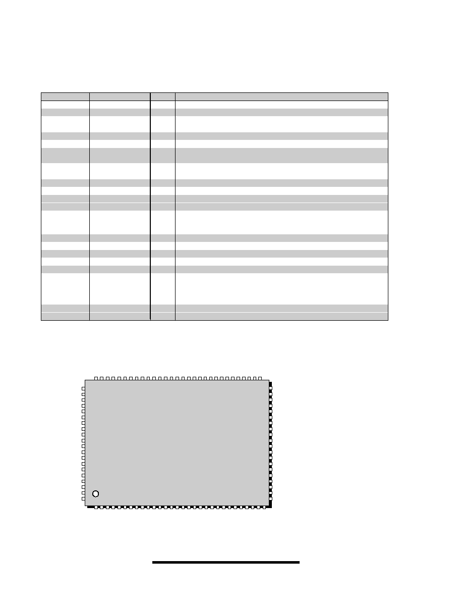
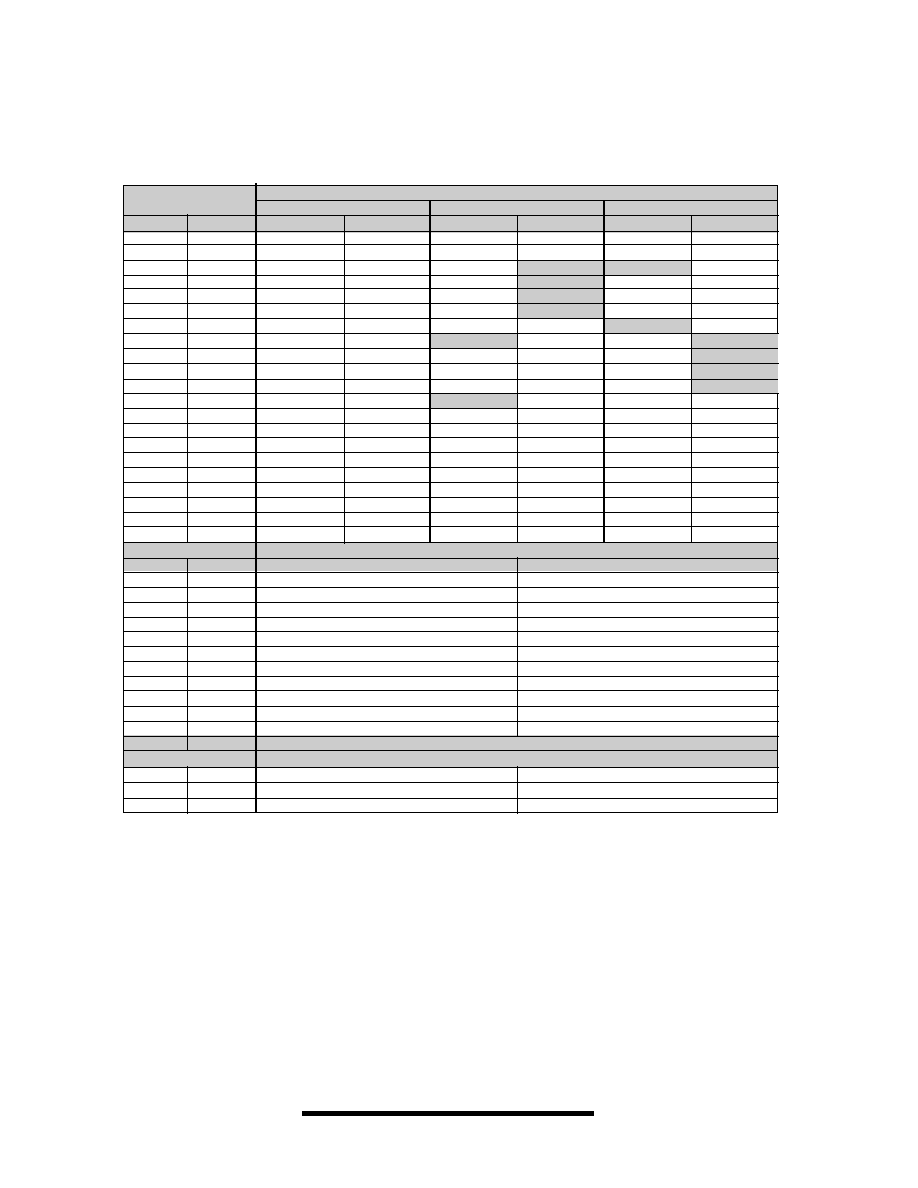
Pin No.(s)
Name(s)
Type
Description
1
BBUS_OEN
O
Asserts when DATA7-0 (B bus) is enabled for output
2,3,5,6,7,9,10,11
DATA15-8
I/O
Upper 8 bits of bidirectional three-state data bus for transfer of commands, data, and status
between TNT4882 and CPU ≠ also known as the A bus
14
ABUSN
I
Enables register accesses through the A bus (DATA15-8) ≠ DATA15 is the most significant bit
19-15
ADDR4-0
I
Determines which register to access during a read or write operation
20
ABUS_OEN
O
Asserts when DATA15-8 (A bus) is enabled for output
21
TADCS
O
Asserts when the TNT4882 is an active or addressed IEEE 488 Talker (TADS, TACS, or SPAS)
22
CPUACC
O
Asserts in two-chip mode during a NAT4882 register I/O access
23
TRIG
O
Asserts when in DTAS or when the auxiliary trigger software command is issued
26
PAGED
I
Asserting this pin pages in the page-in registers in the 7210 mode
28
REM
O
Asserts when the TNT4882 is in a remote state (REMS or RWLS)
29
SWAPN
I
Rearranges the order of the registers when asserted and in 9914 mode
30
FIFO_RDY
O
Asserts when the FIFO is ready for burst access
31
BURST_RDN
I
When asserted, places the TNT4882 in a burst read mode, in which the first word in the
FIFO is always driven on the TNT4882 data bus ≠ words are removed from the FIFOs at
each rising edge of RDN ≠ see reference manual for details
32
DRQ
O
Asserts to request a DMA transfer cycle
33
DACKN
I
Enables FIFO accesses during a DMA transfer cycle
34
INTR
O
Asserts when one or more of the unmasked interrupt conditions becomes true
38
RDY1
O
Asserts during an I/O access to indicate that the read data is available or that the write
data has been latched ≠ asserts immediately on an access to Turbo488 registers or in
one-chip mode
50,49,47,46,
DATA7-0
I/O
Lower eight bits of bidirectional three-state data bus for transfer of commands, data, and
44,43,42,39
status between TNT4882 and CPU ≠ also known as the B bus ≠ DATA7 is the most significant bit
Generic Pin Description
All pins with names that end in `N' are active low; all others are active high. All input (I) and bidirectional (I/O) pins have an internal pull-up
resistor between 50 k
and 150 k
.
Note: You can also see the "Hardware Considerations" chapter of the "TNT Programmer Reference Manual" (P/N 320724-01) for more
information.
TNT4882
Single-Chip IEEE 488.2 Talker/Listener ASIC
National Instruments
Phone: (512) 794-0100 ∑ Fax: (512) 683-9300 ∑ info@natinst.com ∑ www.natinst.com
4
Pin No.(s)
Name(s)
Type
Description
51
DCAS
O
Asserts when the device clear state machine is in DCAS
52
NC
O
Leave this pin unconnected
53
MODE
I
Determines whether the TNT4882 powers up in 7210 or 9914 emulation mode ≠
High = 7210 mode, Low = 9914 mode
55
CSN
I
Chip Select enables I/O transfers between the CPU and the TNT4882
62
BBUSN
I
Enables register accesses through the B bus (DATA7-0)
63
RDN
I
Enables the contents of the registers selected by ADDR 4:0 and CSN or the FIFOs to
appear on the data bus selected by ABUSN and BBUSN
64
WRN
I
Latches data on the bus selected by ABUSN and BBUSN into an internal TNT4882 register
on the trailing (rising) edge of WRN
66
LADCS
O
Asserts when the TNT4882 is addressed as a Listener
67
RESETN
I
Holds the TNT4882 in its idle state
71,74,77,80,88,
DIO8-1N
I/O
8-bit bidirectional IEEE 488 data bus
89,91,92
70,73,76,79,
RENN, ATNN, SRQN,
I/O
IEEE 488 control signals
81,82,84,85
IFCN, NDACN, NRFDN,
DAVN, EOIN
95
XTAL0
O
Output of crystal circuit ≠ use only for driving a quartz crystal
96
XTAL1
I
Crystal oscillator input ≠ drive with a 40 MHz CMOS input level clock signal
98
KEYCLKN
O
Strobes data to or from a DS1204 electronic key
99
KEYDQ
I/O
Transmits serial data between the TNT4882 and a DS1204 key
100
KEYRSTN
O
Resets a DS1204 key
4,8,13,25,27,35,37
GND
_
Ground pins ≠ 0 V
41,45,48,54,56,57,
59,61,65,68,72,75,
78,83,86,90,93,97
12,24,36,40,58,
VDD
_
Power pins ≠ +5 V (±5%)
60,69,87,94
DIO6N
GND
IOCS16N
DIO8N
GND
IFCN
DIO5N
SRQN
GND
DIO7N
ATNN
RENN
GND
RESET
80 79 78 77 76 75 74 73 72
84
85
86
87
88
89
90
91
92
93
94
95
96
97
98
99
100
1
2
3
4
5
6
7
8
9 10 11 12 13 14 15 16 17
71 70 69 68 67 66 65 64
31
32
33
34
35
36
37
38
39
40
41
42
43
44
45
46
47
GND
DATA5
DATA4
GND
AEN_N
VDD
GND
DATA0
INTR
DACKN
DRQ
ADDR9
DAVN
GND
VDD
GND
DIO2N
DIO1N
DIO3N
VDD
XTAL1
EOIN
IOWN
GND
VDD
SW7
SW6
NC
D15_8_OEN
ADDR4
ADDR3
ADDR2
ADDR1
ADDR0
BHEN_N
ADDR5
GND
ADDR6
ADDR7
ADDR8
TNT4882
ISA Pin Configuration
DIO4N
GND
XTAL0
GND
KEYCLKN
KEYDQ
KEYRSTN
DATA3
DATA2
DATA1
GND
VDD
IOCHRDY
VDD
18 19 20 21 22 23 24 25 26 27 28 29 30
DATA10
GND
DATA11
DATA12
DATA13
GND
DATA14
DATA15
D7_0_OEN
DATA9
DATA8
VDD
GND
48
GND
49
DATA6
50
DATA7
63
IORN
62
SENSE_8_16N
61
GND
60
VDD
59
VDD
58
VDD
57
GND
56
VDD
55
SW5
54
NC
53
MODE
52
SW9
51
SW8
83
GND
82
NRFDN
81
NDACN
ISA Pin Configuration
Figure 4. TNT4882 ISA Pin Configuration
Table continued from page 3
TNT4882
Single-Chip IEEE 488.2 Talker/Listener ASIC
National Instruments
Phone: (512) 794-0100 ∑ Fax: (512) 683-9300 ∑ info@natinst.com ∑ www.natinst.com
5
ISA Pin Description
All input (I) and bidirectional (I/O) pins have an internal pull-up resistor between 50 k
and 150 k
. Pins with names that end in "N" are
active low signals ≠ all others are active high. Open-collector outputs are type "OC."
Note: You can also see the "Hardware Considerations" chapter of the "TNT Programmer Reference Manual" (P/N 320724-01) for more
information.
Pin No.(s)
Name(s)
Type
Description
1
D7_0_OEN
O
Asserts when DATA7-0 bus is enabled for output ≠ may be left unconnected
2,3,5,6,7,9,10,11
DATA15-8
I/O
Upper eight bits of bidirectional three-state data bus for transfer of commands,
data, and status between TNT4882 and CPU ≠ can connect directly to the AT bus ≠
DATA15 is the most significant bit
14
BHEN_N
I
Enables access to upper eight bits of data bus when asserted
19-15
ADDR4-0
I
Determines which register will be accessed during an I/O access
31,30,29,28,26
ADDR9-5
I
Determines if an I/O address is within the range occupied by the TNT4882 ≠
the chip is selected and an I/O access occurs when ADDR9-5 match SW9-5 and
AEN_N is asserted
20
D15_8_OEN
O
Asserts when DATA15:8 bus is enabled for output ≠ may be left unconnected
21,54
NC
O
Leave unconnected
52,51,23,22,55
SW9-5
I
Determines the base address of the TNT4882
32
DRQ
O
Asserts to request a DMA transfer cycle
33
DACKN
I
Enables FIFO accesses during a DMA transfer cycle
34
INTR
O
Asserts when one or more of the unmasked interrupt conditions becomes true
37
AEN_N
I
Enables I/O accesses to the TNT4882
38
IOCHRDY
OC
When the TNT4882 is not accessed, this open-collector signal is not driven, and a
pull-up resistor on the system board keeps it pulled high ≠ at the start of some
TNT4882 accesses, the TNT4882 may drive it low, then pull it high again during the
cycle to indicate that the TNT4882 is ready for the CPU to end that cycle
50,49,47,46,44,
DATA7-0
I/O
Lower eight bits of bidirectional three-state data bus for transfer of commands, data,
43,42,39
and status between TNT4882 and CPU ≠ can connect directly to the AT bus ≠ DATA7
is the most significant bit
53
MODE
I
Forces the TNT4882 to 7210 (high) or 9914 (low) emulation mode on a hardware
reset ≠ may be left unconnected
62
SENSE_8_16N
I
Pull this pin low to tell the TNT4882 that it is connected to a 16-bit bus ≠ leave it
unconnected if the TNT4882 is connected to an 8-bit bus
63
IORN
I
Drives the contents of the register selected by ADDR4-0 on the data bus when the
TNT4882 is selected
64
IOWN
I
The value on the data bus is latched into the register selected by ADDR4-0 on the
rising edge of IOWN when you select the TNT4882
66
IOCS16N
OC
Driven low during an access to the upper data bus
67
RESET
I
Causes a hardware reset and holds the TNT4882 in its idle state while asserted
71,74,77,80,88,
DIO8-1N
I/O
8-bit bidirectional IEEE 488 data bus
89,91,92
70,73,76,79,81,
RENN, ATNN, SRQN,
I/O
IEEE 488 control signals
82,84,85
IFCN, NDACN, NRFDN,
DAVN, EOIN
95
XTAL0
O
Output of crystal circuit ≠ use only for driving a quartz crystal
96
XTAL1
I
Crystal oscillator input ≠ drive with a 40 MHz CMOS input level clock signal
98
KEYCLKN
O
Strobes data to or from the DS1204 electronic key
99
KEYDQ
I/O
Transmits serial data between the TNT4882 and a DS1204 key
100
KEYRSTN
O
Resets a DS1204 key
4,8,13,25,27,35,41,
GND
≠
Ground pins ≠ 0 V
45,48,57,61,65,68,72,
75,78,83,86,90,93,97
12,24,36,40,56,58,
VDD
≠
Power pins ≠ +5 V (±5%)
59,60,69,87,94
TNT4882
Single-Chip IEEE 488.2 Talker/Listener ASIC
National Instruments
Phone: (512) 794-0100 ∑ Fax: (512) 683-9300 ∑ info@natinst.com ∑ www.natinst.com
6
TNT4882 Register Map
Notes on Register Map
1. For complete register descriptions, see the "TNT4882
Programmer Reference Manual" (320724-01)
2. Some of the 7210 mode registers, such as the ISR1, have
the same names as some of the 9914 mode registers. The
7210 mode registers are NOT the same as their 9914 mode
counterparts. Be sure to refer to the appropriate bit map for
the chip emulation mode you are using when programming
these registers.
3. The shaded registers are "paged-in registers." Paged-in
registers only exist in 9914 mode. Writing to the address of the
9914 mode ADSR normally does not access any registers.
Writing one of four page-in commands to the AUXCR changes
all subsequent writes to that address to that of the
corresponding paged-in register. The two readable paged-in
registers, the 9914 mode SPSR and ISR2, are both paged in
whenever any one of the four writable paged-in registers is
paged in. When you write the clear page-in command to the
AUXCR, all paged-in registers are paged out again and are no
longer accessible.
4. There are several unused bytes in the address space of the
TNT4882. These addresses are reserved for adding new
features to the chip. You should not map any external
hardware into these addresses or access them at any time, as
this may cause compatibility problems with future versions of
the TNT4882.
NAT4882 Registers
7210 Mode
9914 Mode
9914 Mode Swapped
ADDR4-0
Hex Offset
Read Register
Write Register
Read Register
Write Register
Read Register
Write Register
00000
0
DIR
CDOR
ISR0
IMR0
DIR
CDOR
00010
2
ISR1
IMR1
ISR1
IMR1
CPTR
PPR
00100
4
ISR2
IMR2
ADSR
IMR2
SPSR
SPMR
"
"
EOSR
"
"
BCR
"
"
ACCR
00110
6
SPSR
SPMR
BSR
AUXCR
ISR2
ADR
01000
8
ADSR
ADMR
ISR2
ADR
ADSR
IMR2
"
"
EOSR
"
"
BCR
"
"
ACCR
01010
A
CPTR
AUXMR
SPSR
SPMR
BSR
AUXCR
01100
C
ADR0
ADR
CPTR
PPR
ISR0
IMR0
01110
E
ADR1
EOSR
DIR
CDOR
ISR1
IMR1
10001
11
DSR
SH_CNT
≠
≠
≠
≠
10011
13
≠
HIER
≠
≠
≠
≠
10101
15
≠
MISC
≠
≠
≠
≠
10111
17
CSR
KEYREG
≠
≠
≠
≠
11011
1B
SASR
DCR
≠
≠
≠
≠
11101
1D
ISR0
IMR0
≠
≠
≠
≠
11111
1F
BSR
BCR
≠
≠
≠
≠
Turbo488 Registers (Same in All Modes)
ADDR4-0
Hex Offset
Read Register
Write Register
01001
9
CNT2
CNT2
01011
B
CNT3
CNT3
01101
D
≠
HSSEL
10000
10
STS1
CFG
10010
12
IMR3
IMR3
10100
14
CNT0
CNT0
10110
16
CNT1
CNT1
11000
18
FIFOB
FIFOB
11001
19
FIFOA
FIFOA
11010
1A
ISR3
CCR
11100
1C
STS2
CMDR
11110
1E
TIMER
TIMER
Special Registers Only Accessible in ISA Pin Configuration
ADDR4-0
Hex Offset
Read Register
Write Register
00101
5
≠ ACCWR
00111
7
≠ INTR
TNT4882
Single-Chip IEEE 488.2 Talker/Listener ASIC
National Instruments
Phone: (512) 794-0100 ∑ Fax: (512) 683-9300 ∑ info@natinst.com ∑ www.natinst.com
7
NC
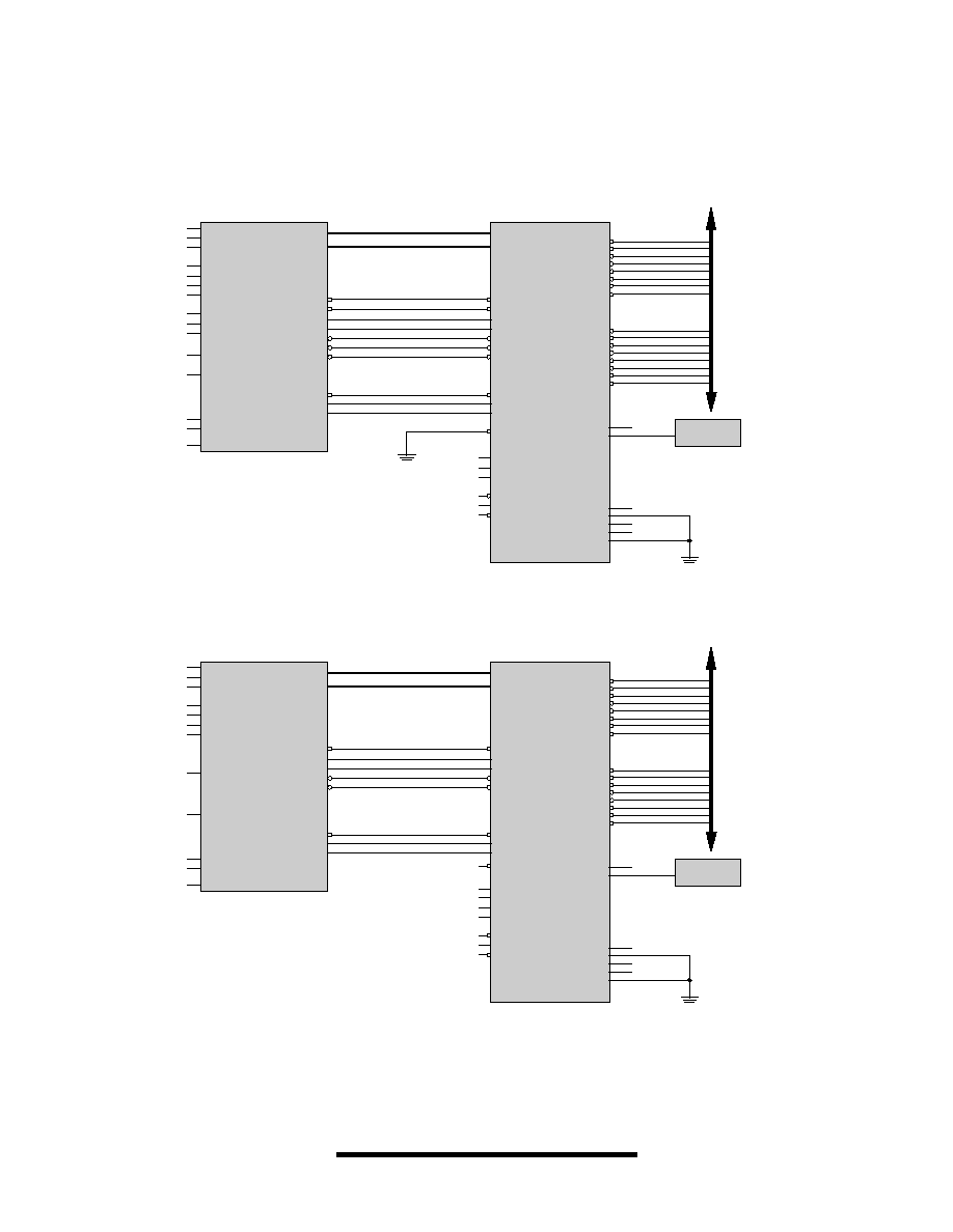
AT(ISA) Bus
Connector
TNT4882
DIO7N
DIO1N
GPIB
NDACN
IFCN
NC
NC
NC
NC
NC
NC
NC
NC
NC
NC
NC
NC
NC
NC
BALE
SA19-16
LA23-17
SMEMR*
SMEMW*
MEMR*
MEMW*
MEMCS16*
NOWS*
REFRESH*
MASTER16*
IOCHK*
BCLK
OSC
TC
Connect DACKN, DRQ, and
INTR to one of the available
lines on the AT bus.
SD15-0
SA9-0
SBHE*
AEN
IOCHRDY
RESET
IOW*
IOR*
IOCS16*
DACK*7-5
DRQ7-5
IRQ (3-7,9,10-12,14,15)
DATA15-0
ADDR9-0
BHEN_N
AEN_N
IOCHRDY
RESET
IOWN
IORN
IOCS16N
DACKN
DRQ
INTR
SENSE_8_16N
NC
NC
NC
NC
NC
NC
D15_8_OEN
D7_0_OEN
MODE
KEYRSTN
KEYDQ
KEYCLKN
DIO8N
DIO2N
DIO3N
DIO4N
DIO5N
DIO6N
RENN
NRFDN
DAVN
EOIN
ATNN
SRQN
40 MHz CMOS
OSCILLATOR
XTAL0
XTAL1
SW9
SW8
SW7
SW6
SW5
NC
NC
NC
NC
}
The TNT4882 is selected when
the binary value on these pins
matches that on ADDR9-5.
Connecting them to ground
causes the corresponding
address lines to be compared to
zero; leaving them unconnected
causes those address lines to be
compared to one. (Base I/O
address 2C0 hex shown.)
NC
PC/XT Bus
Connector
TNT4882
DIO7N
DIO1N
GPIB
NDACN
IFCN
NC
NC
NC
NC
NC
NC
NC
NC
NC
NC
NC
BALE
SA19-16
LA23-17
SMEMR*
SMEMW*
MEMR*
MEMW*
REFRESH*
IOCHK*
BCLK
OSC
TC
Connect DACKN, DRQ, and
INTR to one of the available
lines on the PC bus.
SD7-0
SA9-0
AEN
IOCHRDY
RESET
IOW*
IOR*
DACK*3-1
DRQ3-1
IRQ7-2
DATA7-0
ADDR9-0
AEN_N
IOCHRDY
RESET
IOWN
IORN
DACKN
DRQ
INTR
SENSE_8_16N
NC
NC
NC
NC
NC
NC
D15_8_OEN
D7_0_OEN
MODE
KEYRSTN
KEYDQ
KEYCLKN
DIO8N
DIO2N
DIO3N
DIO4N
DIO5N
DIO6N
RENN
NRFDN
DAVN
EOIN
ATNN
SRQN
40 MHz CMOS
OSCILLATOR
XTAL0
XTAL1
SW9
SW8
SW7
SW6
SW5
NC
NC
NC
NC
}
The TNT4882 is selected
when the binary value on
these pins matches that on
ADDR9-5. Connecting
them to ground causes the
corresponding address lines
to be compared to zero;
leaving them unconnected
causes those address lines
to be compared to one. (Base
I/O address 2C0 hex shown.)
NC
NC
DATA15-8
Figure 5. PC/XT and AT (ISA) Bus to ISA Mode TNT4882
Hardware Interfacing ≠ ISA Mode TNT4882

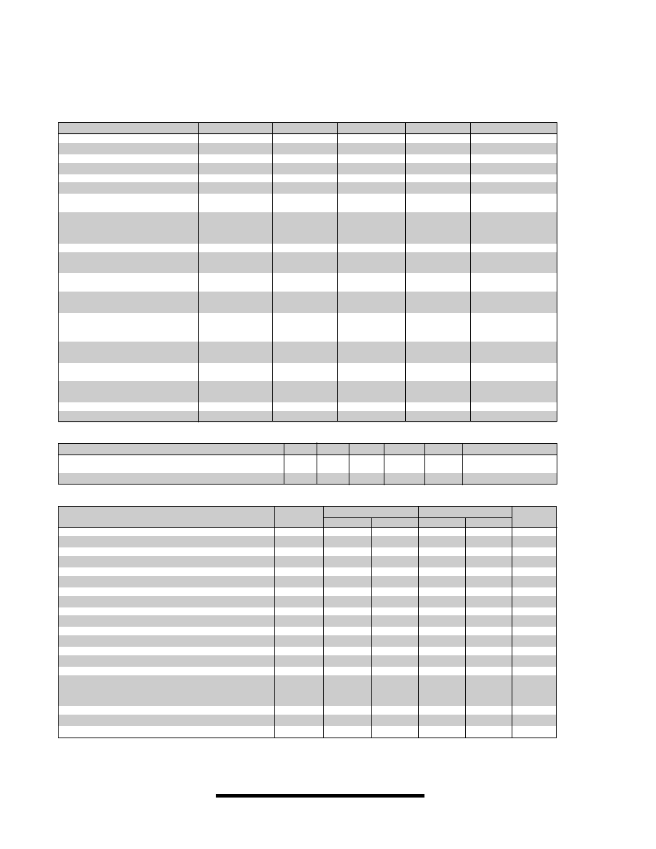
TNT4882
Single-Chip IEEE 488.2 Talker/Listener ASIC
National Instruments
Phone: (512) 794-0100 ∑ Fax: (512) 683-9300 ∑ info@natinst.com ∑ www.natinst.com
8
SENSE_8_16N
BHEN_N
ADDR4-0
IORN
IOWN
DATA15-8
DATA7-0
0
0
11000
0
1
FIFOA
FIFOB
0
0
11000
1
0
FIFOA
FIFOB
0
0
XXXX1
0
1
Read
Not Driven
0
0
XXXX1
1
0
Written
Ignored
0
1
XXXX0
0
1
Not Driven
Read
0
1
XXXX0
1
0
Ignored
Written
1
1
XXXX0
0
1
Not Driven
Read
1
1
XXXX0
1
0
Ignored
Written
1
1
XXXX1
0
1
Not Driven
Read
1
1
XXXX1
1
0
Ignored
Written
ISA Pin Configuration Byte Lane Table
This table shows which byte lane accesses the TNT4882 internal
registers during an I/O access when you use the ISA pin
configuration. All combinations of ADDR4-1, SENSE_8_16N,
and BHEN_N not shown in this table are illegal. You should not
apply these combinations to the TNT4882 while the chip is
selected. The accessed register is determined only by ADDR4-0,
not SENSE_8_16N or BHEN_N.

TNT4882
Single-Chip IEEE 488.2 Talker/Listener ASIC
National Instruments
Phone: (512) 794-0100 ∑ Fax: (512) 683-9300 ∑ info@natinst.com ∑ www.natinst.com
9
Generic Pin Configuration Byte Lane Table
This table shows which byte lanes will access TNT4882 registers
during I/O accesses.
Figure 6. Intel CPU to Generic Mode TNT4882
74245
CPU (80186)
TNT4882-AQ
(GENERIC)
GPIB
74573
NC
NC
NC
NC
NC
NC
40 MHz CMOS
OSCILLATOR
NC
NC
NC
NC
DIO8N
DIO7N
DIO6N
DIO5N
DIO4N
DIO3N
DIO2N
DIO1N
RENN
NDACN
NRFDN
DAVN
EOIN
ATNN
SRQN
IFCN
XTAL0
XTAL1
KEYRSTN
KEYDQ
KEYCLKN
TADCS
LADCS
REM
TRIG
DCAS
ABUS_OEN
BBUS_OEN
NC
NC
NC
NC
NC
NC
AD0
DRQ
WRN
DACKN
DATA7-0
RESETN
BBUSN
ADDR4-0
ABUSN
INTR
CSN
CPUACC
PAGED
SWAPN
BURST_RDN
FIFO_RDY
MODE
RRN
RDY1
DATA15-8
DRQ0
ARDY
RD
BHE
INT0
ALE
DEN
AD15-0
WR
RESET
DT/R
73245
Decode
Hardware Interfacing ≠ Generic Mode TNT4882
ABUSN
BBUSN
ADDR4-0
D15-8
D7-0
0
1
11000
FIFOB
unused
1
0
11000
unused
FIFOB
0
0
11000
FIFOA
FIFOB
0
1
XXXXX*
used
unused
1
0
XXXXX*
unused
used
*Any address except 11000
TNT4882
Single-Chip IEEE 488.2 Talker/Listener ASIC
National Instruments
Phone: (512) 794-0100 ∑ Fax: (512) 683-9300 ∑ info@natinst.com ∑ www.natinst.com
10
Generic Mode DC Characteristics
Parameter
Symbol
Min
Max
Unit
Notes
Supply voltage
V
DD
4.75 5.25
V
Voltage input low
V
IL
-0.5 0.8
V
Voltage input high
V
IH
2.0
V
CC
V
Voltage output low
V
OL
0.0
0.4
V
Voltage output high
V
OH
2.4
V
DD
V
Supply current
I
DD
90
mA
50 mA, typical
Output current low
I
OL
24
mA
V
OL
= 0.4 V
DATA15-0, LADCS, DRQ, INTR, RDY1
Output current low
I
OL
8
mA
V
OL
= 0.4 V
BBUS_OEN, ABUS_OEN, TADCS,
CPUACC, REM, TRIG, DCAS, CIC
FIFO_RDY
I
OL
4
mA
V
OL
= 0.4 V
Output current low
I
OL
2
mA
V
OL
= 0.4 V
KEYDQ, KEYRSTN, KEYCLKN
DIO8-1N, IFCN, SRQN, EOIN, ATNN,
I
OL
48
mA
V
OL
= 0.4 V
RENN, DAVN, NRFDN, NDACN
Output current high
I
OH
-12
mA
V
OH
= V
DD
-0.5 V
DATA15-0, LADCS, DRQ, INTR, RDY1
-24
mA
V
OH
= 2.4 V
Output current high
I
OH
-4
mA
V
OH
= V
DD
-0.5 V
BBUS_OEN, ABUS_OEN, TADCS,
CPUACC, REM, TRIG, DCAS
-8
mA
V
OH
= 2.4 V
FIFO_RDY
I
OH
-2
mA
V
OH
= V
DD
-0.5 V
-4
V
OH
= 2.4 V
Output current high
I
OH
-1
mA
V
OH
= V
DD
-0.5 V
KEYDQ, KEYRSTN, KEYCLKN
-2
mA
V
OH
= 2.4 V
DIO8-1N, IFCN, SRQN, EOIN, ATNN,
I
OH
16
mA
V
OH
= 2.4 V
RENN, DAVN, NRFDN, NDACN
Input leakage current ≠ all pins
I
IH
±10
µ
A
V
DD
= 5.5 V
Output leakage current ≠ all pins
I
OZ
±10
µ
A
V
DD
= 5.5 V
Generic Mode Capacitance
Parameter
Symbol
Min
Typ
Max
Unit
Notes
Pin capacitance
C
50
pF
DIO8-1N, RENN, ATNN, IFCN, SRQN, DAVN, EOIN, NDACN, NRFDN
Pin capacitance all other pins
C
3.6
pF
Generic Mode AC Characteristics
Commercial
Industrial
Parameter
Symbol
Min
Max
Min
Max
Unit
Address setup to RDN = 0, WRN = 0
t
AS
24
27
ns
Data delay from RDN = 0, CSN = 0 (one-chip mode access)
t
RD
71
78
ns
Data float from RDN = 1
t
DF
40
44
ns
RDN pulsewidth (I/0 access)
t
RW
71
78
ns
RDN recovery width
t
RR
40
44
ns
Address hold from RDN = 1, WRN = 1
t
AH
0
0
ns
DRQ unassertion
t
DU
78
86
ns
Data delay from RDN = 0, DACKN = 0
t
DR
40
44
ns
Data setup to WRN = 1
t
WS
14
16
ns
Data hold from WRN = 1
t
WH
0
0
ns
CSN setup to RDN or WRN
t
CS
0
0
ns
CSN hold from RDN or WRN
t
CH
0
0
ns
DACKN setup to RDN or WRN
t
DS
0
0
ns
DACKN hold from RDN or WRN
t
DH
0
0
ns
RDN or WRN to CPUACC (two-chip mode NAT4882 access only)
t
CPU
26
29
ns
RDN or WRN to RDY1 assert
t
ARDY
Two-chip mode NAT4882 access
10
10
clock periods
Other accesses
25
28
ns
RDN or WRN to RDY1 unassert
t
URDY
22
25
ns
WRN pulse width (DMA access)
t
WP
40
44
ns
RDN pulse width (DMA access)
t
RP
40
44
ns

TNT4882
Single-Chip IEEE 488.2 Talker/Listener ASIC
National Instruments
Phone: (512) 794-0100 ∑ Fax: (512) 683-9300 ∑ info@natinst.com ∑ www.natinst.com
11
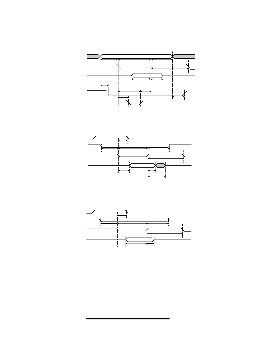
Figure 8. DMA Read
Figure 7. CPU Read
Figure 9. CPU Write
Generic Mode AC Characteristics Waveforms
Waveforms continued on page 12
DATA
WRN
CSN
ABUSN,
BBUSN,
ADDR4-0
t
AS
t
CS
t
WH
t
CH
t
AH
t
WS
t
WP
t
CPU
t
URDY
t
ARDY
t
CPU
RDY1
CPUACC
CPUACC asserts during two-chip mode
NAT4882 accesses only
DRQ
DACKN
RDN
DATA15-0
t
DU
t
DR
t
DS
t
DH
t
DF
RDY1
t
RDYQ
t
URDY
t
RP
ABUSN,
BBUSN,
ADDR4-0
t
AS
t
AH
CSN
t
CS
t
CH
RDN
DATA
t
DF
t
RD
t
URDY
t
CPU
t
ARDY
t
RW
t
CPU
RDY1
CPUACC
CPUACC asserts during two-chip mode
NAT4882 accesses only

TNT4882
Single-Chip IEEE 488.2 Talker/Listener ASIC
National Instruments
Phone: (512) 794-0100 ∑ Fax: (512) 683-9300 ∑ info@natinst.com ∑ www.natinst.com
12
WRN
DRQ
DACKN
DATA15-0
t
WS
t
WH
t
DU
t
DS
t
DH
Figure 10. DMA Write
Waveforms continued from page 11
ISA Mode DC Characteristics
Parameter
Symbol
Min
Max
Unit
Notes
Supply voltage
V
DD
4.75 5.25
V
Voltage input low
V
IL
-0.5 0.8
V
Voltage input high
V
IH
2.0
V
CC
V
Voltage output low
V
OL
0.0
0.4
V
Voltage output high
V
OH
2.4
V
DD
V
Supply current
I
DD
90
mA
50 mA, typical
Output current low
I
OL
24
mA
V
OL
= 0.4 V
DATA15-0
DRQ, INTR, IOCS16, IOCHRDY
Output current low
I
OL
16
mA
V
OL
= 0.4 V
D7_0_OEN
Output current low
I
OL
8
mA
V
OL
= 0.4 V
D15_8_OEN, TP_INTWTN
Output current low
I
OL
2
mA
V
OL
= 0.4 V
KEYDQ, KEYRSTN, KEYCLKN
Output current low
DIO8-1N, RENN, ATNN, IFCN, SRQN,
I
OL
48
mA
V
OL
= 0.4 V
DAVN, EOIN, NDACN, NRFDN
Output current high
I
OH
-12
mA
V
OH
= V
DD
-0.5 V
DATA15-0
DRQ, INTR
-24
mA
V
OH
= 2.4 V
Output current high
I
OH
-8
mA
V
OH
= V
DD
-0.5 V
D7_0_OEN
-16
mA
V
OH
= 2.4 V
Output current high
I
OH
-4
mA
V
OH
= V
DD
-0.5 V
D15_8_OEN,
TP_INTWTN
-8
mA
V
OH
= 2.4 V
Output current high
I
OH
-1
mA
V
OH
= V
DD
-0.5 V
KEYDQ, KEYRSTN,
KEYCLKN
-2
mA
V
OH
= 2.4 V
Output current high
DIO8-1N, RENN, ATNN, IFCN, SRQN,
I
OH
-16
mA
V
OH
= 2.4 V
DAVN, EOIN, NDACN, NRFDN
Input leakage current ≠ all pins
I
IH
±10
mA
V
DD
= 5.5 V
Output leakage current ≠ all pins
I
OZ
±10
mA
V
DD
= 5.5 V
TNT4882
Single-Chip IEEE 488.2 Talker/Listener ASIC
National Instruments
Phone: (512) 794-0100 ∑ Fax: (512) 683-9300 ∑ info@natinst.com ∑ www.natinst.com
13
Figure 11. I/O Read Access
Waveforms continued on page 14
ISA Mode Capacitance
Parameter
Symbol
Min
Typ
Max
Unit
Notes
Pin capacitance
C
3.6
pF
DATA15-0, DRQ, INTR, IOCS16N,
IOCHRDY, ADDR6
Pin capacitance
C
3.0
pF
D7_0_OEN, D15_8_OEN, TP_INTWTN,
KEYDQ, KEYRSTN, KEYCLKN, ADDR4,
ADDR8, ADDR9
Pin capacitance
C
3.5
pF
BHEN_N, ADDR3-0, ADDR5, ADDR7,
DACKN, AEN_N, MODE, TESTMODE,
PWBSEL2-0, SW9, SENSE_8_16N,
IORN, IOWN, RESET
Pin capacitance
C
50
pF
DIO8-1N, RENN, ATNN, IFCN, SRQN,
DAVN, EOIN, NDACN, NRFDN
Parameter
Symbol
Min
Max
Unit
Notes
ADDR9-0 setup to IORN, IOWN
t
AS
30
ns
ADDR9-0 hold from IORN, IOWN
t
AH
0
ns
DACKN setup to IORN, IOWN
t
DS
0
ns
DACKN hold from IORN, IOWN
t
DH
20
ns
Data setup time to IOWN rising
t
SU
22
ns
Data hold time from IOWN rising
t
WH
0
ns
IORN low pulse width
t
RPWL
100
ns
IORN high pulse width
t
RPWH
42
ns
IOWN low pulse width
t
WPWL
100
ns
IOWN high pulse width
t
WPWH
100
ns
IORN or IOWN held from IOCHRDY
t
TD
20
ns
DRQ unassertion time
t
DU
73
ns
Due to FIFO full/empty
DRQ unassertion time
t
DU
48
ns
Due to byte count reached
Data access time from IORN falling, DMA
t
DACC
80
ns
Data access time from IORN falling, I/O
t
ACC
80
ns
Data hold time from IORN rising
t
RH
0
ns
Data float time from IORN rising
t
DF
30
ns
IOCS16N assertion after valid address
t
DEC
30
ns
IOCS16N negation after invalid address
t
DECN
20
ns
IOCHRDY negation from IORN or IOWN
t
RDYN
40
ns
IOCHRDY release after IORN or IOWN
t
RDY
350
ns
ISA Mode AC Characteristics
ADDR9-0, AEN_N
IORN
DATA15-0
IOCS16N
IOCHRDY
t
AH
t
RH
t
DF
t
DECN
t
TD
t
RDY
t
RDYN
t
ACC
t
DEC
t
AS
t
RPWL
t
RPWH
ISA Mode AC Characteristics Waveforms
TNT4882
Single-Chip IEEE 488.2 Talker/Listener ASIC
National Instruments
Phone: (512) 794-0100 ∑ Fax: (512) 683-9300 ∑ info@natinst.com ∑ www.natinst.com
14
Waveforms continued from page 13
Figure 13. DMA Read Access
Figure 14. DMA Write Access
Figure 12. I/O Write Access
ADDR9-0, AEN_N
IOWN
DATA15-0
IOCS16N
IOCHRDY
t
AH
t
DECN
t
TD
t
RDY
t
RDYN
t
DEC
t
AS
t
WPWL
t
WPWH
t
WH
t
SU
IORN
DRQ
DACKN
DATA15-0
t
DF
t
RH
t
DU
t
DS
t
DH
t
RPWH
t
DACC
t
RPWL
IOWN
DRQ
DACKN
DATA15-0
t
WH
t
DU
t
DS
t
DH
t
WPWH
t
WPWL
t
SU

National Instruments
Phone: (512) 794-0100 ∑ Fax: (512) 683-9300 ∑ info@natinst.com ∑ www.natinst.com
15
TNT4882
Single-Chip IEEE 488.2 Talker/Listener ASIC
Figure 16. Mechanical Data
Figure 17. Recommended Land Pattern (not to scale)
Absolute Maximum Ratings
Property Range
Units
Supply voltage, V
DD
- 0.5 to + 7.0
V
Input voltage, V
IN
- 0.5 to V
CC
+ 0.5
V
Output voltage, V
OUT
- 0.5 to V
CC
+ 0.5
V
Storage temperature, T
STG
- 55 to 150
∞ C
18.85
PIN 1 INDEX
FRONT VIEW
SIDE VIEW
PIN 1
PIN 30
PIN 31
PIN 51
PIN 50
PIN 80
PIN 81
PIN 100
20.00
±
0.10
23.90
±
0.25
0.65
0.22 (MIN)
0.38 (MAX)
12.35
14.00
±
0.10
17.90
±
0.25
3.40 (MAX.)
2.80
±
0.25
0.23
±
0.13
SEE DETAIL A
DETAIL A
0.15
+0.08
≠0.02
0
∞
≠7
∞
0.80
±
0.15
NOTES:
1. All dimensions are shown in millimeters.
2. Unless otherwise specified, all dimensions are nominal.
3. When converting from millimeters to inches, four significant digits
to the right of the decimal point are necessary.
Note:
20 x 30 Lead Pattern
LAND PATTERN
.075
1.90
.013
.330
.745
18.9
.0256
0.65
.980
24.9
PIN 1

TNT4882
Single-Chip IEEE 488.2 Talker/Listener ASIC
Technical Support
National Instruments strives to provide you with quality technical
assistance worldwide. We currently offer electronic technical
support along with our technical support centers staffed by
Applications Engineers.
Access information from our Web site at www.natinst.com
Our FTP site is dedicated to 24-hour support, with a collection of
files and documents to answer your questions. Log on to our
Internet host at ftp.natinst.com
You can fax questions to our Applications Engineers anytime
at (800) 328-2203 or (512) 683-5678. Or, you can call from
8:00 a.m. to 6:00 p.m. (central time) at (512) 795-8248.
Internationally, contact your local office. National Instruments
sponsors a wide variety of group activities, such as user group
meetings at trade shows and at large industrial sites. Our users
also receive our quarterly
Instrumentation Newsletter
TM
with the latest
information on new products, product updates, application tips,
and current events. In addition, sign up for
NI News, our electronic
news service at www.natinst.com/news
Warranty
All National Instruments data acquisition, computer-based
instrument, VXIbus, and MXIbus products are covered by a one-
year warranty. GPIB hardware products are covered by a
two-year warranty from the date of shipment. The warranty
covers board failures, components, cables, connectors, and
switches, but does not cover faults caused by misuse. The owner
may return a failed assembly to National Instruments for repair
during the warranty period. Extended warranties are available
at an additional charge.
Information furnished by National Instruments is believed to
be accurate and reliable. National Instruments reserves the right
to change product specifications without notice.
Seminars/Training
Free and fee-paid seminars are presented several times a year in
cities around the world. Comprehensive, fee-paid training
courses are available at National Instruments offices or at
customer sites. Call for training schedules.
For More Information
Contact National Instruments for Application Notes such as:
"Using the TNT4882 in a MC68340 System"
"Factors to Consider When Clocking the TNT4882 at
Frequencies Less than 40 MHz"
"Porting a 9914 GPIB Design to Use the TNT4882"
Ordering Information
TNT4882-BQ
TNT4882 Developer Kit..........................................776866-01
Includes 2 TNT4882 ASICs, PC AT evaluation board, ESP-488TL
source code software, and documentation.
TNT4882 Programmer Reference Manual ..............320724-01
Part Number Legend
a
b
c
d
e
TNT
4882
B
Q
a. Family name TNT = Single-chip, high-speed,
GPIB Talker/Listener interface
b. Device-number 4882 = IEEE 488.2 compatible
c. Reserved
d. Revision
e. Package type Q = Quad flat pack
U.S. Corporate Headquarters Fax (512) 683-9300 ∑ info@natinst.com
Branch Offices: Australia 03 9879 5166 ∑ Austria 0662 45 79 90 0 ∑ Belgium 02 757 00 20 ∑ Brazil 000 811 781 0559 ∑ Canada 905 785 0085
China 86 21 6555 7838 ∑ Denmark 45 76 26 00 ∑ Finland 09 725 725 11 ∑ France 01 48 14 24 24 ∑ Germany 089 741 31 30 ∑ Hong Kong 2645 3186
India 91805275406 ∑ Israel 03 6120092 ∑ Italy 02 413091 ∑ Japan 03 5472 2970 ∑ Korea 02 596 7456 ∑ Mexico 001 800 010 0793
Netherlands 0348 433466 ∑ New Zealand 09 914 0488 ∑ Norway 32 27 73 00 ∑ Singapore 2265886 ∑ Spain 91 640 0085 ∑ Sweden 08 587 895 00
Switzerland 056 200 51 51 ∑ Taiwan 02 2377 1200 ∑ U.K. 01635 523545
© Copyright 1999 National Instruments Corporation. All rights reserved. Product and company names listed are trademarks or trade names of their respective companies.
0305599
www.natinst.com
(512) 794-0100
*000000A-01*
340570D-01