 | –≠–ª–µ–∫—Ç—Ä–æ–Ω–Ω—ã–π –∫–æ–º–ø–æ–Ω–µ–Ω—Ç: 3240-11 | –°–∫–∞—á–∞—Ç—å:  PDF PDF  ZIP ZIP |

Page 1 of 12
Document No. 70-0034-02
www.psemi.com
©2006 Peregrine Semiconductor Corp. All rights reserved.
Peregrine's PE3240 is a high performance integer-N PLL
capable of frequency synthesis up to 2.2 GHz. The
superior phase noise performance of the PE3240 is ideal
for applications such as wireless local loop basestations,
LMDS systems and other demanding terrestrial systems.
The PE3240 features a 10/11 dual modulus prescaler,
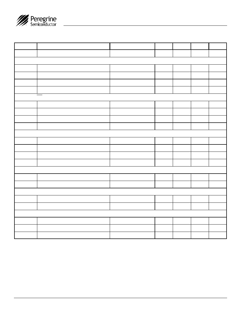
counters and a phase comparator as shown in Figure 1.
Counter values are programmable through a three wire
serial interface.
The PE3240 is manufactured on Peregrine's UltraCMOSTM
process, a patented variation of silicon-on-insulator (SOI)
technology on a sapphire substrate, offering the
performance of GaAs with the economy and integration of
conventional CMOS.
Product Specification
2.2 GHz UltraCMOSTM Integer-N PLL
for Low Phase Noise Applications
Product Description
PE3240
Features
∑
2.2 GHz operation
∑
˜10/11 dual modulus prescaler
∑
Internal phase detector
∑
Serial programmable
∑
Low power--15 mA at 3 V
∑
Ultra-low phase noise
∑
Available in 20-lead TSSOP
Figure 1. Block Diagram
F
in
F
in
Prescaler
10/11
20
Main
Counter
20
Secon-
dary
20-bit
Latch
20
Primary
20-bit
Latch
R Counter
f
r
Phase
Detector
6
6
13
Sdata
PD_U
PD_D

Product Specification
PE3240
Page 2 of 12
©2006 Peregrine Semiconductor Corp. All rights reserved.
Document No. 70-0034-02
UltraCMOSTM RFIC Solutions
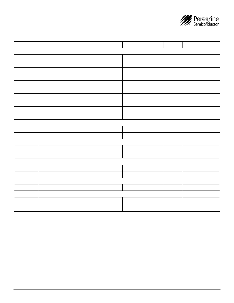
Table 1. Pin Descriptions
Figure 2. Pin Configuration (Top View)
20-lead TSSOP
Figure 3. Package Type
V
DD
1
Enh
2
S_WR
3
Sdata
4
Sclk
5
GND
6
FSELS
7
E_WR
8
V
DD
9
F
in
10
F
in
11
GND
12
Cext
13
LD
14
Dout
15
V
DD
16
PD_D
17
PD_U
18
GND
19
f
r
20
Pin No.
Pin Name
Type
Description
1
V
DD
(Note 1)
Power supply input. Input may range from 2.85 V to 3.15 V. Bypassing required.
2
Enh
Input
Enhancement mode. When asserted low ("0"), enhancement register bits are functional. Internal 70 k
pull-
up resistor.
3
S_WR
Input
Serial load enable input. While S_WR is "low", Sdata can be serially clocked. Primary register data are
transferred to the secondary register on S_WR rising edge.
4
Sdata
Input
Binary serial data input. Input data entered MSB first.
5
Sclk
Input
Serial clock input. Sdata is clocked serially into the 20-bit primary register (E_WR "low") or the 8-bit
enhancement register (E_WR "high") on the rising edge of Sclk.
6
GND
Ground.
7
FSELS
Input
Selects contents of primary register (FSELS=1) or secondary register (FSELS=0) for programming of internal
counters. Internal 70 k
pull-down resistor.
8
E_WR
Input
Enhancement register write enable. While E_WR is "high", Sdata can be serially clocked into the
enhancement register on the rising edge of Sclk. Internal 70 k
pull-down resistor.
9
V
DD
(Note 1)
Same as pin 1.
10
Fin
Input
Prescaler input from the VCO. Max frequency input is 2.2 GHz.
11
F
in
Input
Prescaler complementary input. A bypass capacitor should be placed as close as possible to this pin and be
connected in series with a 50
resistor to the ground plane.
12
GND
Ground.
13
Cext
Output
Logical "NAND" of PD_
U
and PD_
D
terminated through an on chip, 2 k
series resistor. Connecting Cext to
an external capacitor will low pass filter the input to the inverting amplifier used for driving LD.
14
LD
Output
Lock detect is an open drain logical inversion of CEXT. When the loop is in lock, LD is high impedance,
otherwise LD is a logic low ("0").
15
Dout
Output
Data out function, Dout, enabled in enhancement mode.
16
V
DD
(Note 1)
Same as pin 1.

Product Specification
PE3240
Page 3 of 12
Document No. 70-0034-02
www.psemi.com
©2006 Peregrine Semiconductor Corp. All rights reserved.
Table 1. Pin Descriptions (continued)
Pin No.
Pin Name
Type
Description
Note 1: V
DD
pins 1, 9, and 16 are connected by diodes and must be supplied with the same positive voltage level.
Table 2. Absolute Maximum Ratings
Table 3. Operating Ratings
Table 4. ESD Ratings
Electrostatic Discharge (ESD) Precautions
When handling this UltraCMOSTM device, observe
the same precautions that you would use with
other ESD-sensitive devices. Although this device
contains circuitry to protect it from damage due to
ESD, precautions should be taken to avoid
exceeding the specified rating in Table 4.
Latch-Up Avoidance
Unlike conventional CMOS devices, UltraCMOSTM
devices are immune to latch-up.
Note 1: Periodically sampled, not 100% tested. Tested per
MIL-STD-883, M3015 C2
17
PD_
D
Output
PD_
D
pulses down when f
p
leads f
c
.
18
PD_
U
Output
PD_
U
pulses down when f
c
leads f
p
.
19
GND
Ground.
20
f
r
Input
Reference frequency input.
Symbol Parameter/Conditions
Min
Max
Units
V
DD
Supply
voltage
-0.3
4.0 V
V
I
Voltage on any input
-0.3
V
DD
+
0.3
V
I
I
DC into any input
-10
+10
mA
I
O
DC into any output
-10
+10
mA
T
stg
Storage temperature range
-65
150
∞C
Symbol Parameter/Conditions Min Max
Units
V
DD
Supply
voltage
2.85
3.15 V
T
A
Operating ambient
temperature range
-40 85 ∞C
Symbol Parameter/Conditions Level
Units
V
ESD
ESD voltage human body model
(Note 1)
1000 V
Product Specification
PE3240
Page 4 of 12
©2006 Peregrine Semiconductor Corp. All rights reserved.
Document No. 70-0034-02
UltraCMOSTM RFIC Solutions
Table 5. DC Characteristics:
V
DD
= 3.0 V, -40∞ C < T
A
< 85∞ C, unless otherwise specified
Symbol Parameter
Conditions
Min
Typ
Max
Units
I
DD
Operational supply current;
Prescaler enabled
V
DD
= 2.85 to 3.15 V
15
20
mA
Digital Inputs: S_WR, Sdata, Sclk
V
IH
High level input voltage
V
DD
= 2.85 to 3.15 V
0.7 x V
DD
V
V
IL
Low level input voltage
V
DD
= 2.85 to 3.15 V
0.3 x V
DD
V
I
IH
High level input current
V
IH
= V
DD
= 3.15 V
+1
µ
A
I
IL
Low level input current
V
IL
= 0, V
DD
= 3.15 V
-1
µ
A
Digital inputs:
Enh
(contains a 70 k
pull-up resistor)
V
IH
High level input voltage
V
DD
= 2.85 to 3.15 V
0.7 x V
DD
V
V
IL
Low level input voltage
V
DD
= 2.85 to 3.15 V
0.3 x V
DD
V
I
IH
High level input current
V
IH
= V
DD
= 3.15 V
+1
µ
A
I
IL
Low level input current
V
IL
= 0, V
DD
= 3.15 V
-100
µ
A
Digital inputs: FSELS, E_WR (contains a 70 k
pull-down resistor)
V
IH
High level input voltage
V
DD
= 2.85 to 3.15 V
0.7 x V
DD
V
V
IL
Low level input voltage
V
DD
= 2.85 to 3.15 V
0.3 x V
DD
V
I
IH
High level input current
V
IH
= V
DD
= 3.15 V
+100
µ
A
I
IL
Low level input current
V
IL
= 0, V
DD
= 3.15 V
-1
µ
A
Reference Divider input: f
r
I
IHR
High level input current
V
IH
= V
DD
= 3.15 V
+100
µ
A
I
ILR
Low level input current
V
IL
= 0, V
DD
= 3.15 V
-100
µ
A
Counter and phase detector outputs: Dout, PD_
D,
PD_
U
V
OLD
Output
voltage
LOW
I
out
= 6 mA
0.4
V
V
OHD
Output voltage HIGH
I
out
= -3 mA
V
DD
- 0.4
V
Lock detect outputs: (Cext, LD)
V
OLC
Output voltage LOW, Cext
I
out
= 0.1 mA
0.4
V
V
OHC
Output voltage HIGH, Cext
I
out
= -0.1 mA
V
DD
- 0.4
V
V
OLLD
Output voltage LOW, LD
I
out
= 1 mA
0.4
V
Product Specification
PE3240
Page 5 of 12
Document No. 70-0034-02
www.psemi.com
©2006 Peregrine Semiconductor Corp. All rights reserved.
Table 6. AC Characteristics:
V
DD
= 3.0 V, -40∞ C < T
A
< 85∞ C, unless otherwise specified
Note 1: fclk is verified during the functional pattern test. Serial programming sections of the functional pattern are clocked at 10 MHz to verify fclk
specification.
Note 2: CMOS logic levels can be used to drive reference input if DC coupled. Voltage input needs to be a minimum of 0.5 Vp-p. For optimum
phase noise performance, the reference input falling edge rate should be faster than 80mV/ns.
Note 3: Parameter is guaranteed through characterization only and is not tested.
Symbol Parameter
Conditions
Min
Max
Units
Control Interface and Latches (see Figures 6, 7)
f
Clk
Serial data clock frequency
(Note 1)
10
MHz
t
ClkH
Serial clock HIGH time
30
ns
t
ClkL
Serial clock LOW time
30
ns
t
DSU
Sdata set-up time to Sclk rising edge
10
ns
t
DHLD
Sdata hold time after Sclk rising edge
10
ns
t
PW
S_WR pulse width
30
ns
t
CWR
Sclk rising edge to S_WR rising edge
30
ns
t
CE
Sclk falling edge to E_WR transition
30
ns
t
WRC
S_WR falling edge to Sclk rising edge
30
ns
t
EC
E_WR transition to Sclk rising edge
30
ns
Main Divider (Including Prescaler)
F
in
Operating frequency
200
2200
MHz
P
Fin
Input level range
External AC coupling
-5
5
dBm
Main Divider (Prescaler Bypassed)
F
in
Operating frequency
20
220
MHz
P
Fin
Input level range
External AC coupling
-5
5
dBm
Reference Divider
f
r
Operating frequency
(Note 3)
100
MHz
P
fr
Reference input power (Note 2)
Single ended input
-2
dBm
Phase Detector
f
c
Comparison frequency
(Note 3)
20
MHz
SSB Phase Noise (F
in
= 1.3 GHz, f
r
= 10 MHz, f
c
= 1.25 MHz, LBW = 70 kHz, V
DD
= 3.0 V, Temp = -40∞ C
)
100 Hz Offset
-75
dBc/Hz
1 kHz Offset
-85
dBc/Hz