 | –≠–ª–µ–∫—Ç—Ä–æ–Ω–Ω—ã–π –∫–æ–º–ø–æ–Ω–µ–Ω—Ç: 3335-24 | –°–∫–∞—á–∞—Ç—å:  PDF PDF  ZIP ZIP |
Page 1 of 15
Document No. 70-0049-02
www.psemi.com
©2005 Peregrine Semiconductor Corp. All rights reserved.
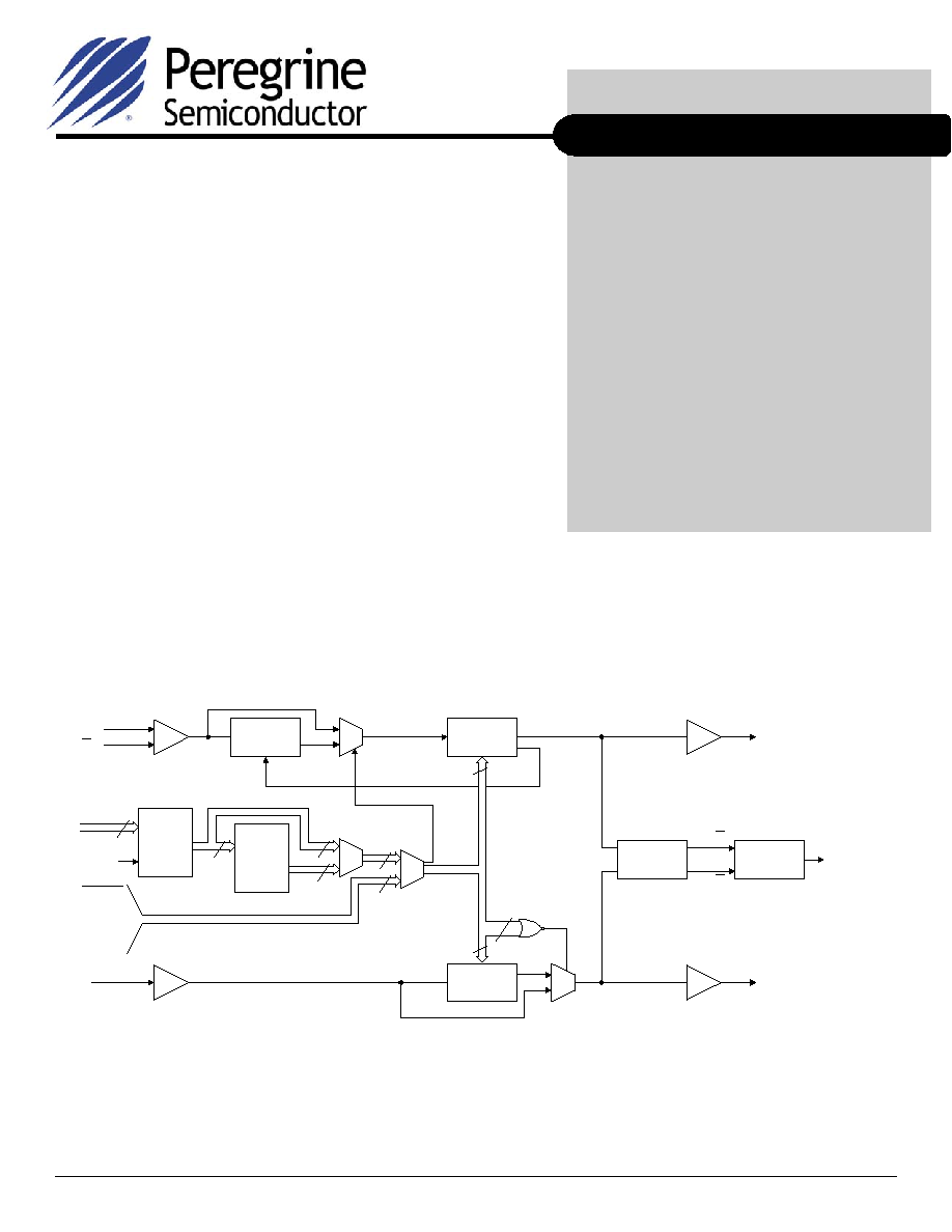
Peregrine's PE3335 is a high performance integer-N PLL
capable of frequency synthesis up to 3000 MHz. The
superior phase noise performance of the PE3335 makes it
ideal for applications such as LMDS / MMDS / WLL
basestations and demanding terrestrial systems.
The PE3335 features a 10/11 dual modulus prescaler,
counters, phase comparator and a charge pump as shown
in Figure 1. Counter values are programmable through
either a serial or parallel interface and can also be directly
hard wired.
The PE3335 Phase Locked-Loop is optimized for terrestrial
applications. It is manufactured on Peregrine's
UltraCMOSTM process, a patented variation of silicon-on-
insulator (SOI) technology on a sapphire substrate, offering
the performance of GaAs with the economy and integration
of conventional CMOS.
Product Specification
3000 MHz UltraCMOSTM Integer-N PLL
for Low Phase Noise Applications
Product Description
PE3335
Features
∑
3000 MHz operation
∑
˜10/11 dual modulus prescaler
∑
Internal phase detector with
charge pump
∑
Serial, parallel or hardwired
programmable
∑
Ultra-low phase noise
∑
Available in 44-lead PLCC and
7x7 mm 48-lead QFN packages
Figure 1. Block Diagram
F
in
F
in
Prescaler
10/11
20
Main
Counter
20
Secon-
dary
20-bit
Latch
20
Primary
20-bit
Latch
Pre_en
M(6:0)
A(3:0)
R(3:0)
16
20
R Counter
f
r
Phase
Detector
6
6
f
c
f
p
8
D(7:0)
13
Sdata
PD_U
PD_D
Charge
Pump
CP
Product Specification
PE3335
Page 2 of 15
©2005 Peregrine Semiconductor Corp. All rights reserved.
Document No. 70-0049-02
UltraCMOSTM RFIC Solutions
Table 1. Pin Descriptions
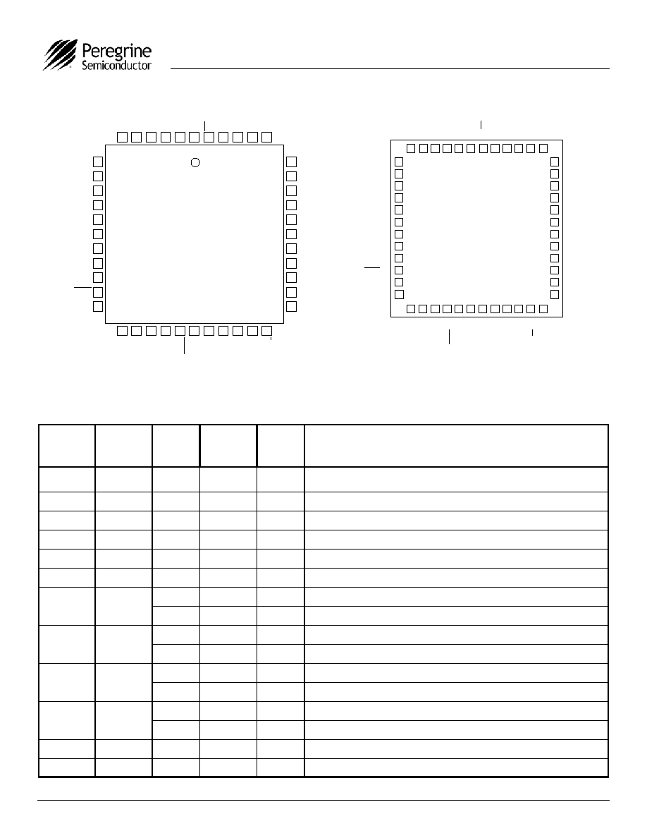
Figure 2. Pin Configurations (Top View)
44-lead PLCC
48-lead QFN
11
12
13
14
15
16
17
10
9
8
7
6
5
4
3
2
1 44 43 42 41 40
35
34
33
32
31
30
29
36
37
38
39
18 19 20 21 22 23 24 25 26 27 28
D
0
, M
0
D
1
, M
1
D
2
, M
2
D
3
, M
3
V
DD
V
DD
S_W R, D
4
, M
4
Sdata, D
5
, M
5
Sclk, D
6
, M
6
FSELS, D
7
, Pre_en
GND
GND
f
p
V
DD
_f
p
D
out
V
DD
C
ext
V
DD
CP
NC
V
DD
_f
c
f
c
F
in
F
in
Ho
p
_
WR
A_
W
R
M1
_
W
R
V
DD
B
m
ode
S
m
ode
,
A
3
M2
_
W
R
,
A
2
E_
W
R
,
A
1
F
SEL
P,
A
0
GN
D
R
3
R
2
R
1
R
0
V
DD
En
h
LD
fr
GN
D
GN
D
GND
R3
R2
R1
R0
V
DD
LD
f
r
GND
GND
D0, M0
D1, M1
D2, M2
D3, M3
V
DD
V
DD
S_W R, D4, M4
Sdata, D5, M5
Sclk, D6, M6
FSELS, D7, Pre_en
GND
47 46 45 44 43 42 41 40 39 38 37
48
5
6
7
8
9
10
11
4
3
2
1
12
13 14 15 16 17 18 19 20 21 22 23 24
31
30
29
28
27
26
25
32
33
34
35
36
Fi
n
Ho
p
_
W
R
A_
W
R
M1
_
W
R
V
DD
B
m
ode
Smo
d
e
,
A3
M2
_
W
R
,
A
2
E_
W
R
,
A1
f
p
V
DD
_f
p
D
out
V
DD
C
ext
V
DD
GND
CP
NC
f
c
FSELP, A0
Fi
n
V
DD
GN
D
V
DD
_f
c
NC
GND
En
h
Pin No.
(44-lead
PLCC)
Pin No.
(48-lead
QFN)
Pin
Name
Interface
Mode
Type Description
1
43
V
DD
ALL
(Note 1)
Power supply input. Input may range from 2.85 V to 3.15 V. Bypassing
recommended.
2
44
R
0
Direct
Input
R Counter bit0 (LSB).
3
45
R
1
Direct
Input
R Counter bit1.
4
46
R
2
Direct
Input
R Counter bit2.
5
47
R
3
Direct
Input
R Counter bit3.
6
48
GND
ALL
(Note 1)
Ground.
7
1
D
0
Parallel
Input
Parallel data bus bit0 (LSB).
M
0
Direct
Input
M Counter bit0 (LSB).
8
2
D
1
Parallel
Input
Parallel data bus bit1.
M
1
Direct
Input
M Counter bit1.
9
3
D
2
Parallel
Input
Parallel data bus bit2.
M
2
Direct
Input
M Counter bit2.
10
4
D
3
Parallel
Input
Parallel data bus bit3.
M
3
Direct
Input
M Counter bit3.
11
5
V
DD
ALL
(Note 1)
Same as pin 1 (QFN48 pin 43).
12
6
V
DD
ALL
(Note 1)
Same as pin 1 (QFN48 pin 43).
Product Specification
PE3335
Page 3 of 15
Document No. 70-0049-02
www.psemi.com
©2005 Peregrine Semiconductor Corp. All rights reserved.
13
7
S_WR
Serial
Input
Serial load enable input. While S_WR is "low", Sdata can be serially clocked.
Primary register data are transferred to the secondary register on S_WR or
Hop_WR rising edge.
D
4
Parallel
Input
Parallel data bus bit4
M
4
Direct
Input
M Counter bit4
14
8
Sdata
Serial
Input
Binary serial data input. Input data entered MSB first.
D
5
Parallel
Input
Parallel data bus bit5.
M
5
Direct
Input
M Counter bit5.
15
9
Sclk
Serial
Input
Serial clock input. Sdata is clocked serially into the 20-bit primary register
(E_WR "low") or the 8-bit enhancement register (E_WR "high") on the rising
edge of Sclk.
D
6
Parallel
Input
Parallel data bus bit6.
M
6
Direct
Input
M Counter bit6.
16
10
FSELS
Serial
Input
Selects contents of primary register (FSELS=1) or secondary register
(FSELS=0) for programming of internal counters while in Serial Interface
Mode.
D
7
Parallel
Input
Parallel data bus bit7 (MSB).
Pre_en
Direct
Input
Prescaler enable, active "low". When "high", F
in
bypasses the prescaler.
17
11
GND
ALL
Ground.
18
12
FSELP
Parallel
Input
Selects contents of primary register (FSELP=1) or secondary register
(FSELP=0) for programming of internal counters while in Parallel Interface
Mode.
A
0
Direct
Input
A Counter bit0 (LSB).
19
13
E_WR
Serial
Input
Enhancement register write enable. While E_WR is "high", Sdata can be
serially clocked into the enhancement register on the rising edge of Sclk.
Parallel
Input
Enhancement register write. D[7:0] are latched into the enhancement register
on the rising edge of E_WR.
A
1
Direct
Input
A Counter bit1.
20
14
M2_WR
Parallel
Input
M2 write. D[3:0] are latched into the primary register (R[5:4], M[8:7]) on the
rising edge of M2_WR.
A
2
Direct
Input
A Counter bit2.
21
15
Smode
Serial,
Parallel
Input
Selects serial bus interface mode (
Bmode=0, Smode=1) or Parallel Interface
Mode (Bmode=0, Smode=0).
A
3
Direct
Input
A Counter bit3 (MSB).
22
16
Bmode
ALL
Input
Selects direct interface mode (
Bmode=1).
23
17,18
V
DD
ALL
(Note 1)
Same as pin 1 (MLP48 pin 43).
24
19
M1_WR
Parallel
Input
M1 write. D[7:0] are latched into the primary register (
Pre_en, M[6:0]) on the
rising edge of M1_WR.
25
20
A_WR
Parallel
Input
A write. D[7:0] are latched into the primary register (R[3:0], A[3:0]) on the
rising edge of A_WR.
26
21
Hop_WR
Serial,
Parallel
Input
Hop write. The contents of the primary register are latched into the
secondary register on the rising edge of Hop_WR.
27
22
F
in
ALL
Input
Prescaler input from the VCO. 3.0 GHz max frequency.
Table 1. Pin Descriptions (continued)
Pin No.
(44-lead
PLCC)
Pin No.
(48-lead
QFN)
Pin
Name
Interface
Mode
Type Description
Product Specification
PE3335
Page 4 of 15
©2005 Peregrine Semiconductor Corp. All rights reserved.
Document No. 70-0049-02
UltraCMOSTM RFIC Solutions
28
23
F
in
ALL
Input
Prescaler complementary input. A bypass capacitor should be placed as
close as possible to this pin and be connected in series with a 50
resistor
directly to the ground plane.
29
24
GND
ALL
Ground.
30
25
f
p
ALL
Output
Monitor pin for main divider output. Switching activity can be disabled through
enhancement register programming or by floating or grounding V
DD
pin 31.
31
26
V
DD
-f
p
ALL
(Note 1)
V
DD
for f
p
. Can be left floating or connected to GND to disable the f
p
output.
32
27
Dout
Serial,
Parallel
Output
Data Out. The MSEL signal and the raw prescaler output are available on
Dout through enhancement register programming.
33
28
V
DD
ALL
(Note 1)
Same as pin 1 (QFN48 pin 43).
34
29
Cext
ALL
Output
Logical "NAND" of PD_
U
and PD_
D
terminated through an on chip, 2 k
series resistor. Connecting Cext to an external capacitor will low pass filter
the input to the inverting amplifier used for driving LD.
35
30
V
DD
ALL
(Note 1)
Same as pin 1 (QFN48 pin 43).
36
32
CP
ALL
Output
Charge pump current is sourced when f
c
leads f
p
and sinked when f
c
lags f
p
.
37
33, 34
NC
ALL
No connection.
38
35
V
DD
-f
c
ALL
(Note 1)
V
DD
for f
c
can be left floating or connected to GND to disable the f
c
output.
39
36
f
c
ALL
Output
Monitor pin for reference divider output. Switching activity can be disabled
through enhancement register programming or by floating or grounding V
DD
pin 38.
40
31,37
GND
ALL
Ground.
41
38,39
GND
ALL
Ground.
42
40
f
r
ALL
Input
Reference frequency input.
43
41
LD
ALL
Output
Lock detect and open drain logical inversion of Cext. When the loop is in lock,
LD is high impedance, otherwise LD is a logic low ("0").
44
42
Enh
Serial,
Parallel
Input
Enhancement mode. When asserted low ("0"), enhancement register bits are
functional.
Table 1. Pin Descriptions (continued)
Note 1: All V
DD
pins are connected by diodes and must be supplied with the same positive voltage level.
V
DD
-f
p
and V
DD
-f
c
are used to power the f
p
and f
c
outputs and can alternatively be left floating or connected to GND to disable the f
p
and f
c
outputs.
Note 2: All digital input pins have 70 k
pull-down resistors to ground.
Pin No.
(44-lead
PLCC)
Pin No.
(48-lead
QFN)
Pin
Name
Interface
Mode
Type Description

Product Specification
PE3335
Page 5 of 15
Document No. 70-0049-02
www.psemi.com
©2005 Peregrine Semiconductor Corp. All rights reserved.
Table 2. Absolute Maximum Ratings
Note 1: Periodically sampled, not 100% tested. Tested per MIL-
STD-883,
M3015
C2
Table 4. ESD Ratings
Electrostatic Discharge (ESD) Precautions
When handling this UltraCMOSTM device, observe
the same precautions that you would use with
other ESD-sensitive devices. Although this device
contains circuitry to protect it from damage due to
ESD, precautions should be taken to avoid
exceeding the specified rating in Table 4.
Latch-Up Avoidance
Unlike conventional CMOS devices, UltraCMOSTM
devices are immune to latch-up.
Table 3. Operating Ratings
Table 5. DC Characteristics:
V
DD
= 3.0 V, -40∞ C < T
A
< 85∞ C, unless otherwise specified
Symbol Parameter/Conditions Min Max Units
V
DD
Supply
voltage
-0.3
4.0 V
V
I
Voltage on any input
-0.3
V
DD
+
0.3
V
I
I
DC into any input
-10
+10
mA
I
O
DC into any output
-10
+10
mA
T
stg
Storage temperature range
-65
150
∞C
Symbol Parameter/Conditions Min Max Units
V
DD
Supply
voltage
2.85
3.15 V
T
A
Operating
ambient
temperature range
-40 85 ∞C
Symbol Parameter/Conditions Level Units
V
ESD
ESD voltage (Human Body
1000
V
Symbol Parameter
Conditions
Min
Typ
Max
Units
I
DD
Operational supply current;
Prescaler disabled
Prescaler enabled
V
DD
= 2.85 to 3.15 V
10
24
31
mA
mA
Digital Inputs: All except f
r
, R
0
, F
in
,
F
in
V
IH
High level input voltage
V
DD
= 2.85 to 3.15 V
0.7 x V
DD
V
V
IL
Low level input voltage
V
DD
= 2.85 to 3.15 V
0.3 x V
DD
V
I
IH
High level input current
V
IH
= V
DD
= 3.15 V
+70
µ
A
I
IL
Low level input current
V
IL
= 0, V
DD
= 3.15 V
-1
µ
A
Reference Divider input: f
r
I
IHR
High level input current
V
IH
= V
DD
= 3.15 V
+100
µ
A
I
ILR
Low level input current
V
IL
= 0, V
DD
= 3.15 V
-100
µ
A
R0 Input (Pull-up Resistor): R
0
I
IHRO
High level input current
V
IH
= V
DD
= 3.15 V
+5
µ
A
I
ILRO
Low level input current
V
IL
= 0, V
DD
= 3.15 V
-5
µ
A
Counter output D
out
V
OLD
Output
voltage
LOW
I
out
= 6 mA
0.4
V
V
OHD
Output voltage HIGH
I
out
= -3 mA
V
DD
- 0.4
V
Lock detect outputs: Cext, LD
V
OLC
Output voltage LOW, Cext
I
out
= 100 mA
0.4
V
V
OHC
Output voltage HIGH, Cext
I
out
= -100 mA
V
DD
- 0.4
V
V
OLLD
Output voltage LOW, LD
I
out
= 6 mA
0.4
V
Charge Pump output: CP
I
CP
- Source
Drive current
V
CP
= V
DD
/ 2
-2.6
-2
-1.4
mA
I
CP
≠ Sink
Drive current
V
CP
= V
DD
/ 2
1.4
2
2.6
mA
I
CPL
Leakage current
1.0 V < V
CP
< V
DD
≠ 1.0 V
-1
1
µ
A
I
CP
≠ Source
vs. I
CP
Sink
Sink vs. source mismatch
VCP = V
DD
/ 2,
T
A
= 25∞ C
15
%
I
CP
vs. V
CP
Output current magnitude variation vs. voltage
V < V
CP
< V
DD
≠ 1.0 V
T
A
= 25∞ C
15
%