 | –≠–ª–µ–∫—Ç—Ä–æ–Ω–Ω—ã–π –∫–æ–º–ø–æ–Ω–µ–Ω—Ç: 3342-06 | –°–∫–∞—á–∞—Ç—å:  PDF PDF  ZIP ZIP |

Page 1 of 17
Document No. 70-0091-03
www.psemi.com
©2005 Peregrine Semiconductor Corp. All rights reserved.
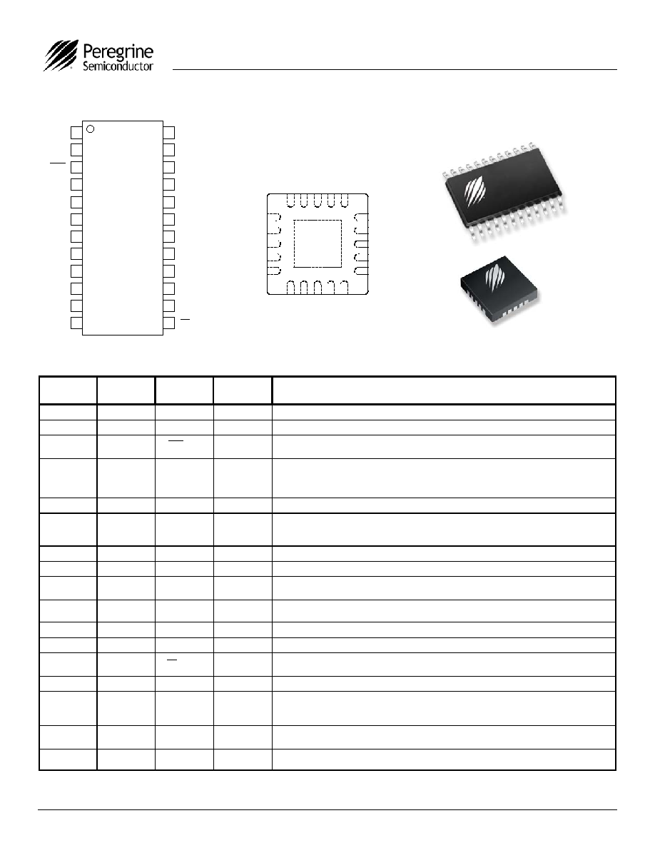
Peregrine's PE3342 is a high performance integer-N PLL with
embedded EEPROM capable of frequency synthesis up to
2700 MHz with a speed-grade option to 3000 MHz. The
EEPROM allows designers to permanently store control bits,
allowing easy configuration of self-starting synthesizers. The
superior phase noise performance of the PE3342 is ideal for
applications such as wireless base stations, fixed wireless, and
RF instrumentation systems.
The PE3342 features a ˜10/11 dual modulus prescaler,
counters, and a phase comparator as shown in Figure 1.
Counter values are programmable through a three-wire serial
interface.
The PE3342 UltraCMOSTM Phase Locked-Loop is
manufactured in Peregrine's patented Ultra Thin Silicon
(UTSiÆ) CMOS process, offering excellent RF performance
with the economy and integration of conventional CMOS.
Product Specification
2.7 GHz Integer-N PLL
with Field-Programmable EEPROM
Product Description
Figure 1. Block Diagram
PE3342
Features
∑
Field-programmable EEPROM for self-
starting applications
∑
Standard 2700 MHz operation,
3000 MHz speed-grade option
∑
˜10/11 dual modulus prescaler
∑
Internal phase detector
∑
Serial programmable
∑
Low power -- 20 mA at 3 V
∑
Ultra-low phase noise
∑
Available in 24-lead TSSOP or 20-lead
4x4 mm QFN package
Enhancement
Register
(8-bit)
F
in
F
in
Prescaler
˜10/11
M Counter
˜2 to ˜512
20
20
Serial
Interface
Mux
R Counter
˜1 to ˜64
f
r
Phase
Detector
6
S_WR
PD_U
PD_D
V
PP
EELoad
EESel
FSel
Clock
Data
20
LD
Cext
Primary
Register
(20-bit)
EE
Register
(20-bit)
Transfer
Logic
EEPROM
ENH
E_WR
13
6
Secondary
Register
(20-bit)
2k
Product Specification
PE3342
Page 2 of 17
©2005 Peregrine Semiconductor Corp. All rights reserved.
Document No. 70-0091-03
UltraCMOSTM RFIC Solutions
Table 2. Pin Descriptions
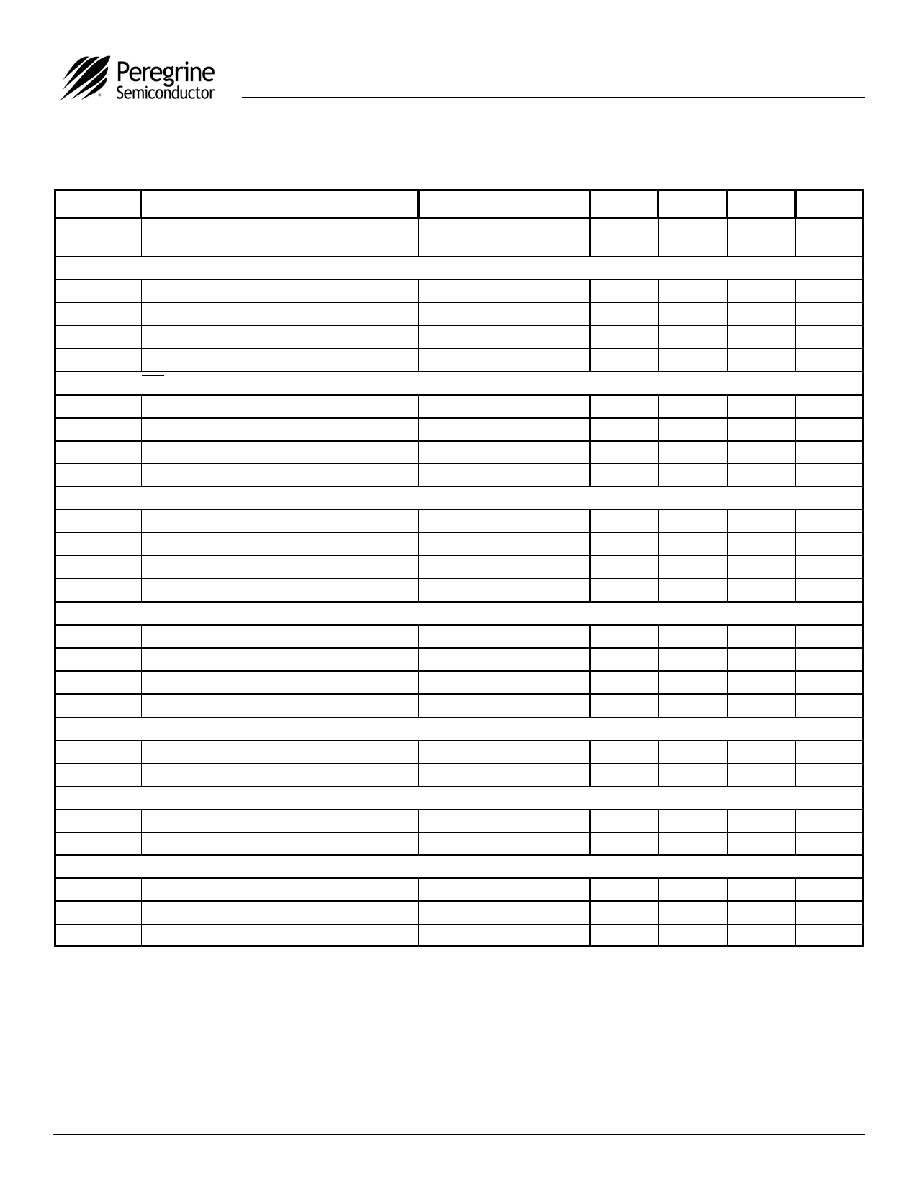
Figure 2. Pin Configurations (Top View)
Figure 3. Package Types
24-lead TSSOP, 20-lead QFN
Pin No.
TSSOP
Pin No.
QFN
Pin Name
Type
Description
1
19
V
DD
(Note 1)
Power supply input. Input may range from 2.85 V to 3.15 V. Bypassing required.
2
GND
(Note 2)
Ground.
3
20
ENH Input
Enhancement mode control line. When asserted LOW, enhancement register bits are
functional. Internal 70 k
pull-up resistor.
4
1
S_WR
Input
Secondary Register WRITE input. Primary Register contents are copied to the
Secondary Register on S_WR rising edge. Also used to control Serial Port operation
and EEPROM programming.
5
2
Data
Input
Binary serial data input. Input data entered LSB (B
0
) first.
6
3
Clock
Input
Serial clock input. Data is clocked serially into the 20-bit Primary Register, the 20-bit
EE Register, or the 8-bit Enhancement Register on the rising edge of Clock. Also used
to clock EE Register data out Dout port.
7
GND
(Note 2)
Ground.
8
4
FSel
Input
Frequency Register selection control line. Internal 70 k
pull-down resistor.
9
5
E_WR
Input
Enhancement Register write enable. Also functions as a Serial Port control line.
Internal 70 k
pull-down resistor.
10
6
V
PP
Input
EEPROM erase/write programming voltage supply pin. Requires a 100pF bypass
capacitor connected to GND.
11
7
V
DD
(Note 1)
Same as pin 1.
12
8
F
in
Input
Prescaler input from the VCO.
13
9
F
in
Input
Prescaler complementary input. A series 50
resistor and DC blocking
capacitor
should be placed as close as possible to this pin and connected to the ground plane.
14
GND
(Note 2)
Ground.
15
10
C
EXT
Output
Logical "NAND" of PD_
U
and PD_
D
terminated through an on-chip, 2 k
series
resistor.
Connecting C
EXT
to an external capacitor will low pass filter the input to the
inverting amplifier used for driving LD.
16
11
EELoad
Input
Control line for Serial Data Port, Frequency Register selection, EE Register parallel
loading, and EEPROM programming. Internal 70 k
pull-down resistor.
17
12
LD
Output, OD
Lock detect output, an open-drain logical inversion of C
EXT
. When the loop is in lock,
LD is high impedance; otherwise, LD is a logic LOW.
V
PP
V
DD
F
IN
F
IN
X
C
EXT
1
20
19
18
17
16
15
14
13
12
11
6
7
8
9
10
2
3
4
5
20-lead QFN
4x4mm
Exposed Solder Pad
(Bottom Side)
S_WR
Data
Clock
FSel
E_WR
EELoad
LD
Dout
V
DD
PD_D
PD
_
U
EE
Se
l
f
r
V
DD
EN
H
V
DD
S_WR
Data
Clock
GND
FSel
E_WR
V
PP
F
in
24-lead TSSOP
EELoad
LD
Dout
V
DD
PD_D
PD_U
GND
f
r
ENH
15
16
17
18
19
20
21
22
23
24
10
9
8
7
6
5
4
3
2
1
GND
F
in
13
14
12
11
GND
V
DD
Cext
EESel

Product Specification
PE3342
Page 3 of 17
Document No. 70-0091-03
www.psemi.com
©2005 Peregrine Semiconductor Corp. All rights reserved.
18
13
Dout
Output
Data out function. Dout is defined with the Enhancement Register and enabled with
ENH
.
19
14
V
DD
(Note 1)
Same as pin 1.
20
15
PD_
D
Output
Phase detector output. PD_D pulses negatively when fp leads fc.
21
16
PD_
U
Output
Phase detector output. PD_U pulses negatively when fc leads fp.
22
17
EESel
Input
Control line for Frequency Register selection, EE Register parallel loading, and
EEPROM programming. Internal 70 k
pull-up resistor.
23
GND
(Note 2)
Ground.
24
18 f
r
Input
Reference frequency input.
Table 3. DC Electrical Specifications
Pin No.
TSSOP
Pin No.
QFN
Pin Name
Type
Description
Notes 1: V
DD
pins 1, 11, and 19 (TSSOP) or pins 6, 14 and 19 (QFN), are connected by diodes and must be supplied with the same positive voltage
level.
2: Ground connections are made through the exposed solder pad. The solder pad must be soldered to the ground plane for proper operation
.
Table 2. Absolute Maximum Ratings
Symbol Parameter/Conditions Min
Max Units
V
DD
Supply voltage
≠0.3
+4.0 V
V
I
Voltage on any digital
input
≠0.3
V
DD
+0.3
V
T
Stg
Storage temperature
range
≠65
+85
∞C
Symbol Parameter/Conditions Min
Max Units
V
DD
Supply
voltage
2.85 3.15 V
T
A
Operating
ambient
temperature range
-40 85 ∞C
Symbol
Parameter/Conditions Min Max Units
V
ESD
ESD voltage human body
model (Note 1)
1000
V
V
ESD
(V
PP
)
ESD voltage human body
model (Note 1)
200
V
Note 1: Periodically sampled, not 100% tested. Tested per MIL-
STD-883, M3015 C2
Table 4. ESD Ratings
Electrostatic Discharge (ESD) Precautions
When handling this UltraCMOSTM device, observe
the same precautions that you would use with
other ESD-sensitive devices. Although this device
contains circuitry to protect it from damage due to
ESD, precautions should be taken to avoid
exceeding the specified rating in Table 4.
Latch-Up Avoidance
Unlike conventional CMOS devices, UltraCMOSTM
devices are immune to latch-up.
Absolute Maximum Ratings are those values
listed in the above table. Exceeding these values
may cause permanent device damage.
Functional operation should be restricted to the
limits in the DC and AC Characteristics table.
Exposure to absolute maximum ratings for
extended periods may affect device reliability.
Product Specification
PE3342
Page 4 of 17
©2005 Peregrine Semiconductor Corp. All rights reserved.
Document No. 70-0091-03
UltraCMOSTM RFIC Solutions
Table 5. DC Characteristics
V
DD
= 3.0 V, -40∞ C < T
A
< 85∞ C, unless otherwise specified
Symbol Parameter
Conditions
Min
Typ
Max
Units
I
DD
Operational supply current;
Prescaler enabled
V
DD
= 2.85 to 3.15 V
20
30
mA
Digital Inputs: S_WR, Data, Clock
V
IH
High-level
input
voltage
V
DD
= 2.85 to 3.15 V
0.7 x V
DD
V
V
IL
Low-level input voltage
V
DD
= 2.85 to 3.15 V
0.3 x V
DD
V
I
IH
High-level
input
current
V
IH
= V
DD
= 3.15 V
+1
µ
A
I
IL
Low-level input current
V
IL
= 0, V
DD
= 3.15 V
-1
µ
A
Digital inputs: ENH
,
EESel (contains a 70 k
pull-up resistor)
V
IH
High-level
input
voltage
V
DD
= 2.85 to 3.15 V
0.7 x V
DD
V
V
IL
Low-level input voltage
V
DD
= 2.85 to 3.15 V
0.3 x V
DD
V
I
IH
High-level
input
current
V
IH
= V
DD
= 3.15 V
+1
µ
A
I
IL
Low-level input current
V
IL
= 0, V
DD
= 3.15 V
-100
µ
A
Digital inputs: FSel, EELoad, E_WR (contains a 70 k
pull-down resistor)
V
IH
High-level
input
voltage
V
DD
= 2.85 to 3.15 V
0.7 x V
DD
V
V
IL
Low-level input voltage
V
DD
= 2.85 to 3.15 V
0.3 x V
DD
V
I
IH
High-level
input
current
V
IH
= V
DD
= 3.15 V
+100
µ
A
I
IL
Low-level input current
V
IL
= 0, V
DD
= 3.15 V
-1
µ
A
EE Memory Programming Voltage and Current: V
PP
, I
PP
V
PP
_WRITE
EEPROM write voltage
12.5
V
V
PP
_ERASE
EEPROM erase voltage
-8.5
V
I
PP
_WRITE
EEPROM write cycle current
30
mA
I
PP
_ERASE
EEPROM erase cycle current
-10
mA
Reference Divider input: f
r
I
IHR
High-level
input
current
V
IH
= V
DD
= 3.15 V
+100
µ
A
I
ILR
Low-level input current
V
IL
= 0, V
DD
= 3.15 V
-100
µ
A
Counter output: Dout
V
OLD
Output
voltage
LOW
I
out
= 6 mA
0.4
V
V
OHD
Output voltage HIGH
I
out
= -3 mA
V
DD
- 0.4
V
Lock detect outputs: (C
EXT
, LD)
V
OLC
Output voltage LOW, C
EXT
I
out
= 0.1 mA
0.4
V
V
OHC
Output voltage HIGH, C
EXT
I
out
= -0.1 mA
V
DD
- 0.4
V
V
OLLD
Output voltage LOW, LD
I
out
= 1 mA
0.4
V

Product Specification
PE3342
Page 5 of 17
Document No. 70-0091-03
www.psemi.com
©2005 Peregrine Semiconductor Corp. All rights reserved.
Table 6. AC Characteristics
V
DD
= 3.0 V, -40∞ C < T
A
< 85∞ C, unless otherwise specified
Symbol Parameter
Conditions
Min
Max
Units
Control Interface and Registers (see Figure 4)
f
Clk
Serial data clock frequency
(Note 1)
10
MHz
t
ClkH
Serial clock HIGH time
30
ns
t
ClkL
Serial clock LOW time
30
ns
t
DSU
Data set-up time to Clock rising edge
10
ns
t
DHLD
Data hold time after Clock rising edge
10
ns
t
PW
S_WR pulse width
30
ns
t
CWR
Clock rising edge to S_WR rising edge
30
ns
t
CE
Clock falling edge to E_WR transition
30
ns
t
WRC
S_WR falling edge to Clock rising edge
30
ns
t
EC
E_WR transition to Clock rising edge
30
ns
EEPROM Erase/Write Programming (see Figures 5 & 6)
t
EESU
EELoad rising edge to V
PP
rising edge
500
ns
t
EEPW
V
PP
pulse width
25
30
ms
t
VPP
V
PP
pulse rise and fall times
(Note 2)
1
µ
s
Main Divider (Including Prescaler)
F
In
Operating frequency
300
2700
MHz
F
In
Operating frequency
Speed-grade option (Note 3)
300
3000
MHz
P
FIn
Input level range
External AC coupling
-5
5
dBm
Main Divider (Prescaler Bypassed)
F
In
Operating frequency
(Note 4)
50
270
MHz
P
FIn
Input level range
External AC coupling (Note 4)
-5
5
dBm
Reference Divider
f
r
Operating frequency
(Note 5)
100
MHz
P
fr
Reference input power (Note 4)
Single ended input
-2
dBm
Phase Detector
f
c
Comparison frequency
(Note 6)
20
MHz
SSB Phase Noise (F
in
= 1.3 GHz, f
r
= 10 MHz, f
c
= 1.25 MHz, LBW = 70 kHz, V
DD
= 3.0 V, Temp = -40∞ C
)
100 Hz Offset
-75
dBc/Hz
1 kHz Offset
-85
dBc/Hz
Note 1: f
Clk
is verified during the functional pattern test. Serial programming sections of the functional pattern are clocked at 10 MHz to verify f
Clk
specification.
Note 2: Rise and fall times of the V
PP
programming voltage pulse must be greater than 1
µ
s.
Note 3: The maximum frequency of operation can be extended to 3.0 GHz by ordering a special speed-grade option. Please refer to Table 14,
Ordering Information, for ordering details.
Note 4: CMOS logic levels can be used to drive F
In
input if DC coupled and used in Prescaler Bypass mode. Voltage input needs to be a minimum
of 0.5 Vp-p. For optimum phase noise performance, the reference input falling edge rate should be faster than 80 mV/ns. No minimum
frequency limit exists when operated in this mode.
Note 5: CMOS logic levels can be used to drive reference input if DC coupled. Voltage input needs to be a minimum of 0.5 Vp-p. For optimum
phase noise performance, the reference input falling edge rate should be faster than 80 mV/ns.
Note 6: Parameter is guaranteed through characterization only and is not tested.