 | –≠–ª–µ–∫—Ç—Ä–æ–Ω–Ω—ã–π –∫–æ–º–ø–æ–Ω–µ–Ω—Ç: 4135-02 | –°–∫–∞—á–∞—Ç—å:  PDF PDF  ZIP ZIP |
©2005 Peregrine Semiconductor Corp. All rights reserved.
Page 1 of 9
Document No. 70-0086-04
www.psemi.com
The PE4135 is a high linearity passive Quad MOSFET Mixer
for GSM800 & Cellular Base Station Receivers, exhibiting high
dynamic range performance over a broad LO drive range of up
to 20 dBm. This mixer integrates passive matching networks to
provide single-ended interfaces for the RF and LO ports,
eliminating the need for external RF baluns or matching
networks. The PE4135 is optimized for frequency down-
conversion using low-side LO injection for GSM800 & Cellular
Base Station application, and is also suitable for up-conversion
applications.
The PE4135 is manufactured on Peregrine's UltraCMOSTM
process, a patented variation of silicon-on-insulator (SOI)
technology on a sapphire substrate, offering the performance
of GaAs with the economy and integration of conventional
CMOS.
Product Specification
High Linearity UltraCMOSTM
Quad MOSFET Mixer
Product Description
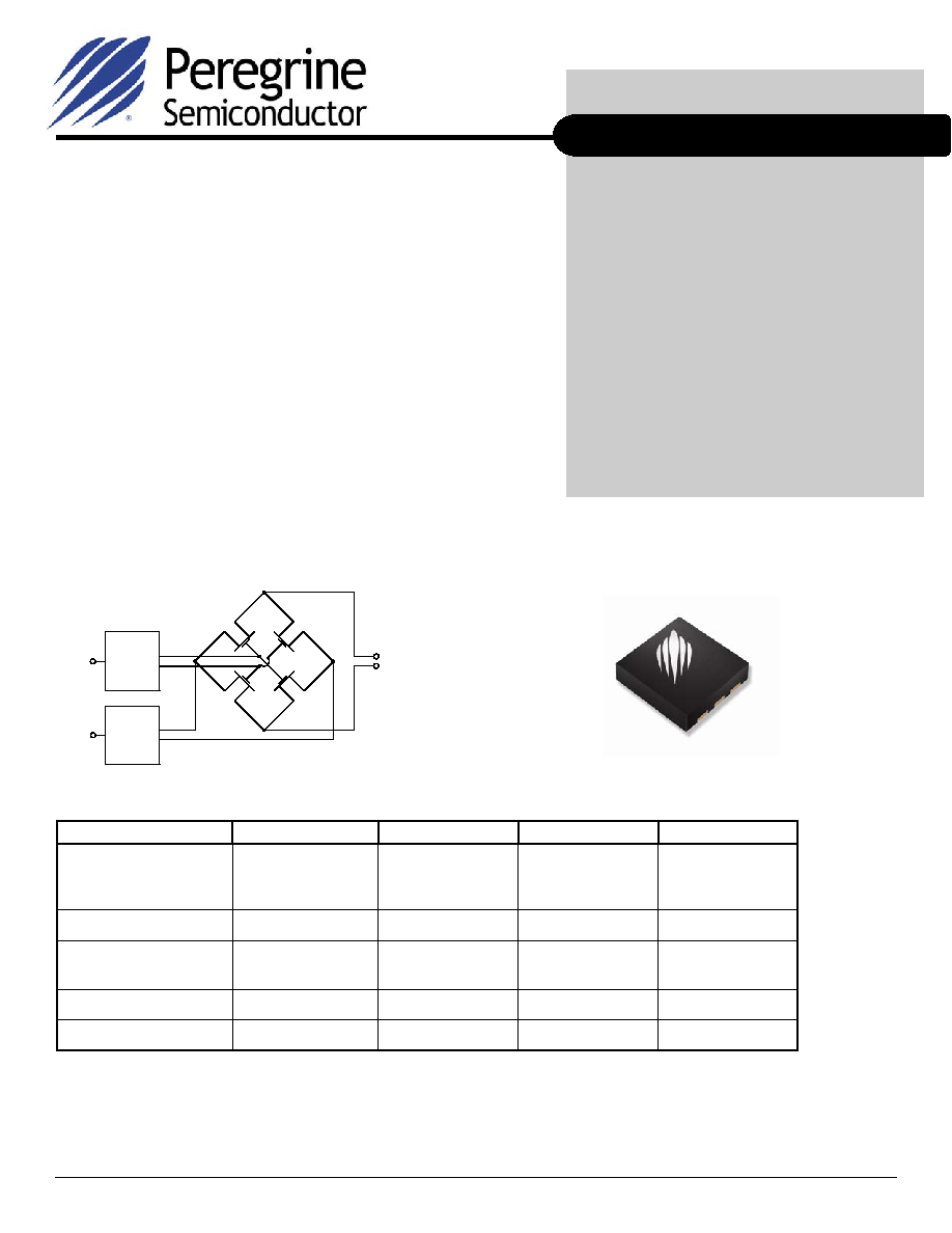
Figure 1. Functional Diagram
PE4135
Features
∑
Integrated, single-ended RF & LO
interfaces
∑
High linearity: Typical IIP3 at 32dBm
820 - 920 MHz (+17 dBm LO)
∑
Low conversion loss: 6.8 dB
(+17 dBm LO)
∑
High isolation: Typical LO-IF at 42 dB,
LO-RF at 32 dB
∑
Small 6-lead 3x3 mm DFN package
Figure 2. Package Type
6-lead DFN
Table 1. Electrical Specifications @ +25 ∞C
Notes:
1. Test conditions unless otherwise noted: IF = 70 MHz, LO input drive = 17 dBm, RF input drive = 3 dBm.
2. An IF frequency of 70 MHz is a nominal frequency. The IF frequency can be specified by the user as long as the RF and LO
frequencies are within the specified maximum and minimum.
3. Conversion Loss includes loss of IF transformer (M/A COM ETC1-1-13, nominal loss 0.7 dB at 70 MHz).
RF
LO
IF
180
o
Two-Way
Power
Divider
180
o
Two-Way
Power
Divider
Parameter
1
Minimum Typical Maximum Units
Frequency Range:
LO
RF
IF
2
750
820
--
--
--
70
850
920
--
MHz
MHz
MHz
Conversion Loss
3
6.8
7.3
dB
Isolation:
LO-RF
LO-IF
30
40
32
42
dB
dB
Input IP3
29
32
dBm
Input 1 dB Compression
21
dBm
©2005 Peregrine Semiconductor Corp. All rights reserved.
Product Specification
PE4135
Page 2 of 9
Document No. 70-0086-04
www.psemi.com
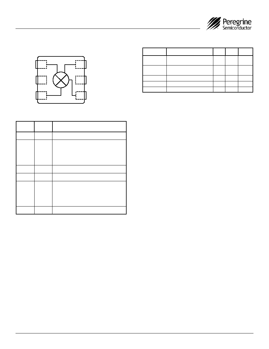
Table 2. Pin Descriptions
Table 3. Absolute Maximum Ratings
Electrostatic Discharge (ESD) Precautions
When handling this UltraCMOSTM device, observe
the same precautions that you would use with
other ESD-sensitive devices. Although this device
contains circuitry to protect it from damage due to
ESD, precautions should be taken to avoid
exceeding the rating specified in Table 3.
Latch-Up Avoidance
Unlike conventional CMOS devices, UltraCMOSTM
devices are immune to latch-up.
Figure 3. Pin Configuration (Top View)
Absolute Maximum Ratings are those values
listed in the above table. Exceeding these values
may cause permanent device damage.
Functional operation should be restricted to the
limits in the DC Electrical Specifications table.
Exposure to absolute maximum ratings for
extended periods may affect device reliability.
PE4135
IF1
GND
LO
IF2
GND
RF
4
5
6
3
2
1
Pin
No.
Pin
Name
Description
1
IF1
IF differential output.
2
GND
Ground connections for Mixer. Traces
should be physically short and connect
immediately to ground plane for best
performance. The exposed solder pad must
also be soldered to the ground plane for
best performance.
3 LO
LO
Input.
4 RF
RF
Input.
5
GND
Ground connections for Mixer. Traces
should be physically short and connect
immediately to ground plane for best
performance. The exposed solder pad must
also be soldered to the ground plane for
best performance.
6
IF2
IF differential output.
Symbol Parameter/Conditions
Min
Max
Units
T
ST
Storage
temperature
range
-65 150 ∞C
T
OP
Operating
temperature
range
-40 85 ∞C
P
LO
LO input power
20
dBm
P
RF
RF input power
12
dBm
V
ESD
ESD Sensitive Device
250
V
Product Specification
PE4135
Page 3 of 9
©2005 Peregrine Semiconductor Corp. All rights reserved.
Document No. 70-0086-04
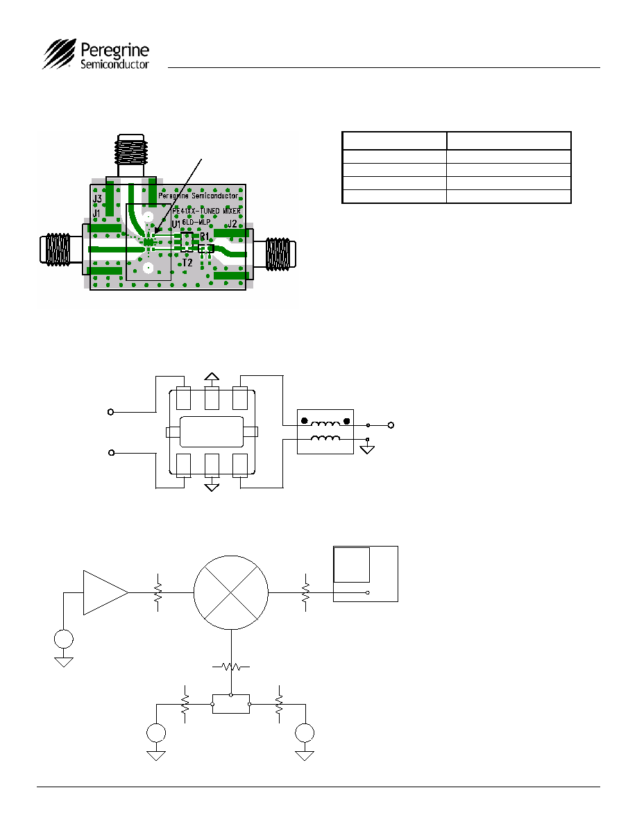
UltraCMOSTM RFIC Solutions
Evaluation Kit
Figure 4. Evaluation Board Layout
Figure 5. Evaluation Board Schematic
4
5
6
3
2
1
RF
LO
IF
T2
6-lead
MLPM
3 x 3 mm
LO
IF
RF
Eval
Board
Sig
Gen
Sig
Gen
Hybrid
Tee
3 dB
PA
Sig
Gen
3 dB
Spectrum
Analyzer
3 dB
6 dB
6 dB
4135
Figure 6. Evaluation Board Testing Block Diagram, 2-Tone Setup
Table 4. Bill of Materials
Reference
Value / Description
T2
M/A Com ETK1-1-13
R1 0
U1
PE4135 MLP Mixer
J1, J2, J3
SMA Connector
Pin 1
©2005 Peregrine Semiconductor Corp. All rights reserved.
Product Specification
PE4135
Page 4 of 9
Document No. 70-0086-04
www.psemi.com
0
5
10
15
20
25
800
850
900
950
1dB
C
o
mpr
e
s
s
i
o
n
(
d
B
)
Frequency (MHz)
-40 C
85 C
25 C
-10
-8
-6
-4
-2
0
800
825
850
875
900
925
950
C
onv
er
s
i
o
n
Los
s
(
d
B
)
Frequency (MHz)
-40 C
25 C
85 C
0
5
10
15
20
25
30
35
40
800
825
850
875
900
925
950
II
P3 (
d
B
m
)
Frequency (MHz)
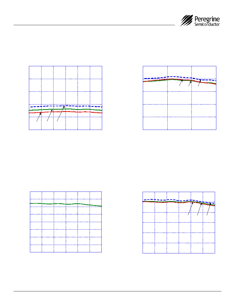
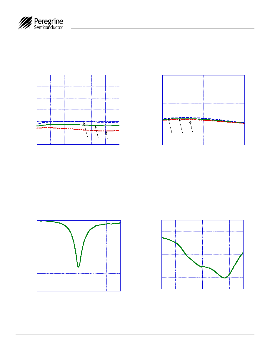
Typical Performance Data (LO=17 dBm, RF=3 dBm, IF=70 MHz)
Figure 8. Input 1dB Compression
Figure 9. Input IP3 @ 25 ∞C
Figure 7. Conversion Loss
Figure 10. Output IP3
0
5
10
15
20
25
30
800
825
850
875
900
925
950
OI
P
3
(d
B
m
)
Frequency (MHz)
-40
8C
85
8C
25
8C
Product Specification
PE4135
Page 5 of 9
©2005 Peregrine Semiconductor Corp. All rights reserved.
Document No. 70-0086-04
UltraCMOSTM RFIC Solutions
-30
-25
-20
-15
-10
-5
0
200
400
600
800
1000
1200
1400
Ret
u
rn
Lo
s
s
(dB
)
Frequency (MHz)
-20
-15
-10
-5
0
200
400
600
800
1000
1200
1400
R
e
t
u
r
n
L
o
ss
(
d
B
)
Frequency (MHz)
-50
-40
-30
-20
-10
0
800
825
850
875
900
925
950
L
O
-
R
F
I
s
o
l
at
i
o
n (d
B
)
Frequency (MHz)
-40 C
85 C
25 C
-60
-50
-40
-30
-20
-10
0
800
825
850
875
900
925
950
L
O
-
I
F
I
s
ol
a
t
io
n
(d
B
)
Frequency (MHz)
-40 C
85 C
25 C
Typical Performance Data (LO=17 dBm, RF=3 dBm, IF=70 MHz)
Figure 12. LO-RF Isolation
Figure 13. LO Port Return Loss @ 25∞C
Figure 11. LO-IF Isolation
Figure 14. RF Port Return Loss @ 25∞C