 | –≠–ª–µ–∫—Ç—Ä–æ–Ω–Ω—ã–π –∫–æ–º–ø–æ–Ω–µ–Ω—Ç: 4257-02 | –°–∫–∞—á–∞—Ç—å:  PDF PDF  ZIP ZIP |
Page 1 of 7
©2005 Peregrine Semiconductor Corp. All rights reserved.
Document No. 70-0166-02
www.psemi.com
4x4mm 20 Lead QFN
RFC
RF1
RF2
CTRL1 CTRL2
CMOS
Control
Driver
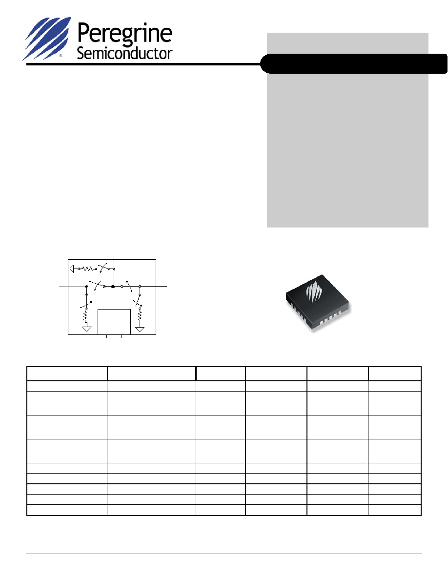
The PE4257 is a high-isolation UltraCMOSTM Switch designed
for wireless applications, covering a broad frequency range
from near DC up to 3000 MHz. This single-supply SPDT
switch integrates a two-pin CMOS control interface. It also
provides low insertion loss with extremely low bias
requirements while operating on a single 3-volt supply. In a
typical wireless application, the PE4257 provides
unprecedented isolation and integration.
The PE4257 is manufactured in Peregrine's patented Ultra
Thin Silicon (UTSiÆ) CMOS process, offering the performance
of GaAs with the economy and integration of conventional
CMOS.
Product Specification
50
SPDT Absorptive UltraCMOSTM
DC ≠ 3.0 GHz RF Switch
Product Description
Figure 1. Functional Diagram
PE4257
Features
∑
50
characteristic impedance
∑
Integrated 50
0.25 watt terminations
∑
High input IP3 > +55 dBm
∑
High isolation 64 dB at 1000 MHz
∑
Low insertion loss: typically 0.75 dB
at 1000 MHz and 0.95 dB at 2000 MHz
∑
LV CMOS two-pin control
∑
Single +3 volt supply operation
∑
Low current consumption: 8
µ
A
Parameter Condition
Minimum
Typical
Maximum
Units
Operating Frequency
1
DC
3000
MHz
Insertion Loss
1000 MHz
2000 MHz
3000 MHz
0.75
0.95
1.2
0.95
1.15
1.4
dB
Isolation Input to Output
1000 MHz
2000 MHz
3000 MHz
61
46
40
64
50
44
dB
Isolation Output to Output
1000 MHz
2000 MHz
3000 MHz
57
54
42
63
60
48
dB
Input IP2
5 MHz - 1000 MHz
80
dBm
Input IP3
5 MHz - 1000 MHz
50
55
dBm
Input 1dB Compression
2
1000 MHz
29
31
dBm
Switching Time
50% CTRL to 10 / 90 RF
2
µs
Video Feedthrough
3
5 MHz - 1000 MHz
15
mV
pp
Notes: 1. Device linearity will begin to degrade below 1 MHz.
2. Note Absolute Maximum ratings in Table 3.
3. Measured with a 1 ns risetime, 0/3 V pulse and 500 MHz bandwidth
Figure 2. Package Type
Table 1. Electrical Specifications @ +25 ∞C, V
DD
= 3.0 V (Z
S
= Z
L
= 50
)

Product Specification
PE4257
Page 2 of 7
Document No. 70-0166-02
UltraCMOSTM RFIC Solutions
©2005 Peregrine Semiconductor Corp. All rights reserved.
4x4mm 20-Lead QFN
GND
15
14
13
12
11
3
4
5
2
1
17
16
18
19
20
9
10
8
7
6
CT
R
L
2
GND
GND
GND
GND
GND
RF
C
VD
D
CT
R
L
1
VSS
/
G
N
D
GND
GND
GND
RF2
GND, RF2 Term.
GND
GND, RF1 Term.
RF1
GND
GND
No. Name
Description
1
GND
RF Ground
2
GND
RF Ground
3
1
RF1
RF I/O
4
GND
RF Ground
5
GND
RF Ground
6
GND
RF Ground
7
GND
RF Ground
8
1
RFC
RF Common
9
GND
RF Ground
10
GND
RF Ground
11
GND
RF Ground
12
GND
RF Ground
13
1
RF2
RF I/O
14
GND
RF Ground
15
GND
RF Ground
16
2
CTRL2
Control 2
17
2
CTRL1
Control 1
18
3
VSS / GND
Negative Supply Option
19
GND
Digital Ground
20
VDD
Supply
Pad
GND
RF Ground Pad
Table 2. Pin Descriptions
Table 3. Absolute Maximum Ratings
Electrostatic Discharge (ESD) Precautions
When handling this UltraCMOSTM device, observe
the same precautions that you would use with
other ESD-sensitive devices. Although this device
contains circuitry to protect it from damage due to
ESD, precautions should be taken to avoid
exceeding the rating specified.
Latch-Up Avoidance
Unlike conventional CMOS devices, UltraCMOSTM
devices are immune to latch-up.
Table 4. DC Electrical Specifications @ 25 ∞C
Notes:
1. RF pins 3, 8, and 13 must be at 0 VDC. The RF pins do not require DC
blocking capacitors for proper operation if the 0 VDC requirement is met.
2. Pins 16 and 17 are the CMOS controls that set the four operating states.
3. Connect pin 18 to GND to enable the negative voltage generator. Connect
pin 18 to V
SS
(-3 V) to bypass and disable internal -3 V supply generator. See
paragraph "Switching Frequency."
Symbol Parameter/Condition Min
Max
Unit
V
DD
Power supply voltage
-0.3
4.0
V
V
I
Voltage on CTRL input
-0.3
V
DD
+
0.3
V
P
RF
RF power on RFC, RF1, RF2
On Port/ Terminated Port
33/24
dBm
T
ST
Storage temperature
-65
+150
∞C
T
OP
Operating temperature
-40
+85
∞C
V
ESD
ESD voltage
(Human Body Model)
1000
V
Parameter Min
Typ
Max
Unit
V
DD
Power Supply
2.7
3.0
3.3
V
I
DD
Power Supply Current
(V
DD
= 3V, V
CNTL
= 3V)
8
20
µA
Control Voltage High
0.70 V
DD
V
Control Voltage Low
0
0.30 V
DD
V
Switching Frequency
The PE4257 has a maximum 25 kHz switching
rate when the internal negative voltage generator
is used (pin 18=GND). The rate at which the
PE4257 can be switched is only limited to the
switching time if an external -3 V supply is
provided at (pin18=V
SS
).
Figure 3. Pin Configuration (Top View)
Absolute Maximum Ratings are those values
listed in the above table. Exceeding these values
may cause permanent device damage.
Functional operation should be restricted to the
limits in the DC Electrical Specifications table.
Exposure to absolute maximum ratings for
extended periods may affect device reliability.
Product Specification
PE4257
Page 3 of 7
©2005 Peregrine Semiconductor Corp. All rights reserved.
Document No. 70-0166-02
www.psemi.com
Table 5. Truth Table
CTRL1
CTRL2
RFC ≠ RF1
RFC ≠ RF2
Low
Low
OFF
OFF
Low
High
OFF
ON
High
Low
ON
OFF
High
High
N/A
1
N/A
1
Product Specification
PE4257
Page 4 of 7
Document No. 70-0166-02
UltraCMOSTM RFIC Solutions
©2005 Peregrine Semiconductor Corp. All rights reserved.
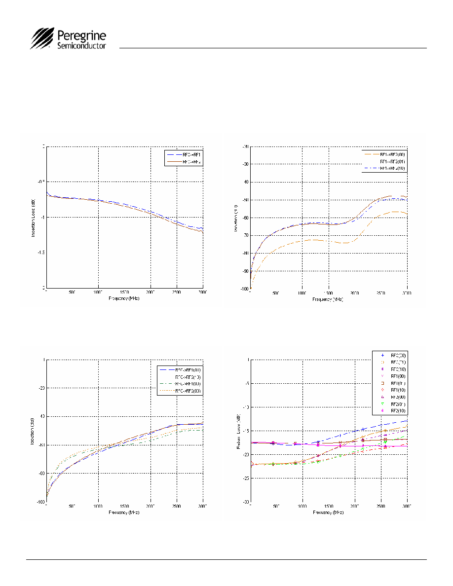
Typical Performance Data @ 25∞C (Unless Otherwise Noted)
(50-ohm impedance)
Figure 4. Insertion Loss ≠ Input - Output
Figure 5. RF1 to RF2 Isolation
Figure 6. Isolation ≠ RFC to RF1/RF2
Figure 7. Return Loss

Product Specification
PE4257
Page 5 of 7
©2005 Peregrine Semiconductor Corp. All rights reserved.
Document No. 70-0166-02
www.psemi.com
Evaluation Kit
The SPDT Switch Evaluation Kit board was designed to
ease customer evaluation of the PE4257 SPDT switch.
The RF common port is connected through a 50
transmission line to J2. Port 1 and Port 2 are
connected through 50
transmission lines to J1 and
J3. A through transmission line connects SMA
connectors J4 and J5. This transmission line can be
used to estimate the loss of the PCB over the
environmental conditions being evaluated.
The board is constructed of a four metal layer FR4
material with a total thickness of 0.031". The
transmission lines were designed using a coplanar
waveguide with ground plane (28 mil core, 47.6 mil
width, 30mil gap).
Note the number of vias surrounding the device in the
layout shown in Figure 8. These vias are critical for
obtaining the specified isolation performance for the
device shown in this datasheet.
J6 provides a means for controlling DC and digital
inputs to the device. The provided jumpers short the
package pin to ground for logic low. When the jumper
is removed, the pin is pulled up to VDD for logic high.
When the jumper is in place, 3 µA of current will flow
through the 1 M
pull up resistor. This extra current
should not be attributed to the requirements of the
device.
Figure 8. Evaluation Board Layouts
Figure 9. Evaluation Board Schematic
Peregrine Specification 101/0151
Peregrine Specification 102/0198