 | –≠–ª–µ–∫—Ç—Ä–æ–Ω–Ω—ã–π –∫–æ–º–ø–æ–Ω–µ–Ω—Ç: 4268-51 | –°–∫–∞—á–∞—Ç—å:  PDF PDF  ZIP ZIP |

©2005 Peregrine Semiconductor Corp. All rights reserved.
Page 1 of 11
Document No. 70-0165-03
www.psemi.com
RX1
RX2
RX3
RX4
TX1
TX2
CMOS
Control/Driver
and ESD
V1
V2
V3
Figure 2. Package Type
20-lead 4x4 mm QFN
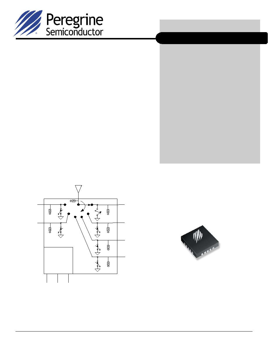
The PE4268 SP6T RF UltraCMOSTM Switch addresses the
specific design needs of the Quad-Band GSM Handset
Antenna Switch Module Market. Broadband performance also
makes it a versatile solution in other IF and RF applications.
The switch includes two high power paths with low insertion
loss and four low power paths with high isolation. On-chip
CMOS decode logic facilitates three-pin low voltage CMOS
control. High ESD tolerance of 1500 V at all ports and no
blocking capacitor requirements make this the ultimate in
integration and ruggedness.
The PE4268 UltraCMOSTM RF Switch is manufactured in
Peregrine's patented Ultra Thin Silicon (UTSiÆ) CMOS
process, offering the performance of GaAs with the economy
and integration of conventional CMOS.
Product Specification
SP6T UltraCMOSTM 2.6 V Switch
100 ≠ 3000 MHz
Product Description
Figure 1. Functional Diagram
PE4268
Features
∑
Three pin CMOS logic control with
integral decoder/driver
∑
Low TX insertion loss: 0.55 dB at 900
MHz, 0.7 dB at 1900 MHz
∑
TX ≠ RX Isolation of 48 dB at 900 MHz,
40 dB at 1900 MHz
∑
Low harmonics: 2f
o
= -84 dBc and
3f
o
= -70 dBc at +35 dBm input power
∑
1500 V HBM ESD tolerance
∑
RX SAW over voltage protection circuit
∑
Harmonics immune to RX VSWR
∑
No blocking capacitors required
∑
20-lead 4x4 mm QFN package

Product Specification
PE4268
Page 2 of 11
©2005 Peregrine Semiconductor Corp. All rights reserved.
Document No. 70-0165-03
UltraCMOSTM RFIC Solutions
Table 1. Electrical Specifications @ +25 ∞C, V
DD
= 2.6 V (Z
S
= Z
L
= 50
)
Parameter Condition
Min
Typ
Max
Unit
Operational Frequency
100
3000
MHz
Insertion Loss
ANT - TX - 850 / 900 MHz
ANT - TX - 1800 / 1900 MHz
ANT - RX - 850 / 900 MHz
ANT - RX - 1800 / 1900 MHz
0.6
0.8
0.9
1.1
0.75
0.95
1.15
1.35
dB
dB
dB
dB
Isolation
TX - RX - 850 / 900 MHz
TX - RX - 1800 / 1900 MHz
TX1 - TX2 - 850 / 900 MHz
TX1 - TX2 - 1800 / 1900 MHz
46
38
28
22
50
42
30
24
dB
dB
dB
dB
Return Loss
850 / 900 MHz
1800 / 1900 MHz
17
15
20
18
dB
dB
2nd Harmonic
1
35 dBm TX Input - 850 / 900 MHz
33 dBm TX Input - 1800 / 1900 MHz
-84
-80
-78
-77
dBc
dBc
3rd Harmonic
1
35 dBm TX Input - 850 / 900 MHz
33 dBm TX Input - 1800 / 1900 MHz
-70
-66
-68
-63
IP3
RX Input
40
dBm
1dB Compression
RX Input
20
dBm
Switching time
(10-90%) (90-10%) RF
2
3
µ
s
dBc
dBc
Note :
1. Harmonics are characterized with a source that is 50
at the fundamental and reflective at the harmonics.
Contact Applications Support at help@psemi.com for more information.

©2005 Peregrine Semiconductor Corp. All rights reserved.
Product Specification
PE4268
Page 3 of 11
Document No. 70-0165-03
www.psemi.com
Table 2. Pin Descriptions
Table 4. Absolute Maximum Ratings
Electrostatic Discharge (ESD) Precautions
When handling this UltraCMOSTM device, observe
the same precautions that you would use with
other ESD-sensitive devices. Although this device
contains circuitry to protect it from damage due to
ESD, precautions should be taken to avoid
exceeding the rating specified in Table 4.
Latch-Up Avoidance
Unlike conventional CMOS devices, UltraCMOSTM
devices are immune to latch-up.
Note 1: ANT port rated higher per applications section, see page 4.
Table 3. DC Electrical Specifications
Table 5. Truth Table
Pin No.
Pin Name
Description
1
1
TX1
RF I/O - TX1
2 GND
Ground
3
1
TX2
RF I/O ≠ TX2
4 GND
Ground
5 GND
Ground
6 VDD
Supply
7
V3
Switch control input, CMOS logic level
8
V2
Switch control input, CMOS logic level
9
V1
Switch control input, CMOS logic level
10 GND
Ground
11
1
RX4
RF I/O - RX4
12
1
RX3
RF I/O - RX3
13 GND
Ground
14
1
RX2
RF I/O - RX2
15
1
RX1
RF I/O - RX1
16 GND
Ground
17 GND
Ground
18 GND
Ground
19
1
ANT
RF Common ≠ Antenna Input
20 GND
Ground
Note 1:
Blocking capacitors needed only when connected to an
external non-zero DC voltage.
Symbol
Parameter/Conditions
Min
Max
Units
V
DD
Power supply voltage
-0.3
4.0
V
V
I
Voltage on any input
-0.3
V
DD
+
0.3
V
T
ST
Storage temperature range
-65
+150
∞C
T
OP
Operating temperature range
-40
+85
∞C
P
IN
TX input power (50
)
+38
dBm
RX input power (50
)
+23
V
ESD
1
ESD Voltage (HBM,
MIL_STD 883 Method
3015.7)
1500
V
ESD Voltage (MM, JEDEC,
JESD22-A114-B)
100
V
ESD Voltage (CDM, JEDEC,
JESD22-C101-A)
2000
V
Parameter
Min
Typ
Max
Units
V
DD
Supply Voltage
2.4
2.6
2.8
V
I
DD
Power Supply Current
(V
DD
= 2.6V)
13
20
µA
Control Voltage High
0.7 x V
DD
V
Control Voltage Low
0.3 x V
DD
V
Path
V3
V2
V1
ANT ≠ RX1
0
0
0
ANT ≠ RX2
0
0
1
ANT ≠ RX3
0
1
0
ANT ≠ RX4
0
1
1
ANT - TX1
1
0
x
ANT - TX2
1
1
x
Figure 3. Pin Configuration (Top View)
Absolute Maximum Ratings are those values
listed in the above table. Exceeding these values
may cause permanent device damage.
Functional operation should be restricted to the
limits in the DC Electrical Specifications table.
Exposure to absolute maximum ratings for
extended periods may affect device reliability.
V
DD
V3
V2
V1
GND
1
20
19
18
17
16
15
14
13
12
11
6
7
8
9
10
2
3
4
5
TX1
GND
TX2
GND
GND
RX4
RX3
GND
RX2
RX1
GND
GND
GND
AN
T
GND
20-lead QFN
4x4mm
Exposed Solder Pad

Product Specification
PE4268
Page 4 of 11
©2005 Peregrine Semiconductor Corp. All rights reserved.
Document No. 70-0165-03
UltraCMOSTM RFIC Solutions
Evaluation Kit
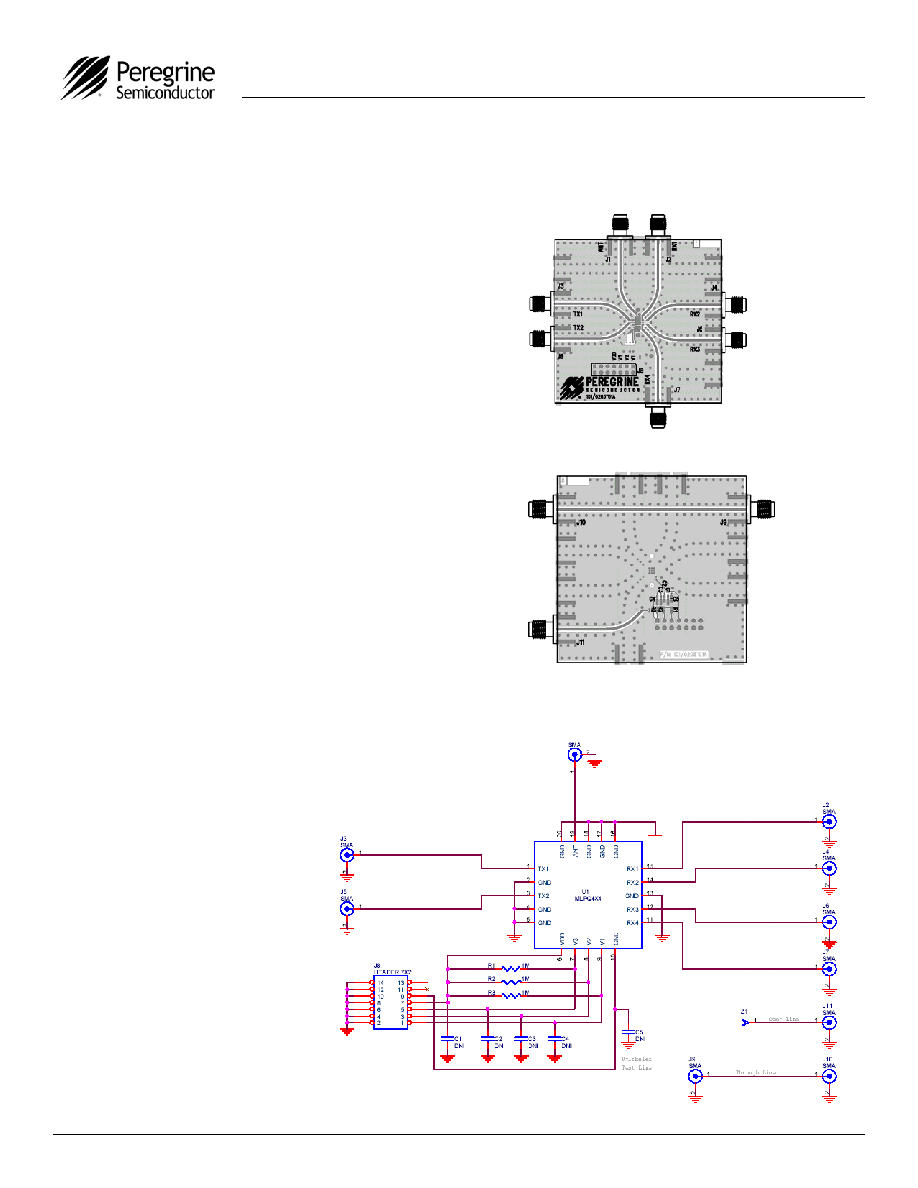
The SP6T Evaluation Kit board was designed to
ease customer evaluation of the PE4268 RF switch.
The PE4268 has two high power TX ports and four
high isolation RX ports. The TX ports are symmetric
and are designed as paths for the 850, 900, 1800, or
1900 MHz bands. The RX ports are also symmetric
and can be assigned to any of these frequency
bands.
The ANT port connects through a 50
transmission
line to the top SMA connector, J1. The RX and TX
ports connect through 50
transmission lines to
SMA connectors J2 ≠ J7. A through 50
transmission line between SMA connectors J9 and
J10 allows estimation of the PCB losses over
environmental conditions. An open transmission line
connected to J11 is also provided.
J8 supplies DC power to the pin marked V
DD
and the
bottom row of pins, which is GND. 1 M
pull-up
resistors are connected from V
DD
to each of the three
control logic inputs: V1, V2, and V3. These pull-up
resistors are provided for ease of evaluation on this
board and are not required for the PE4268 to
operate.
Adding a jumper between a control pin and the
adjacent GND pin on the bottom row of J8 will set a
logic-0 on that control pin. Removing the jumper will
set a logic-1. To evaluate the PE4268, add or
remove jumpers according to the truth table in
Table 5.
Figure 4. Evaluation Board Layout
ANT RX1
RX2
RX3
RX4
TX1
TX2
Open Line
Through-Line
Figure 5. Evaluation Board Schematic
Peregrine Specification 101/0205
Peregrine Specification 102/0267

©2005 Peregrine Semiconductor Corp. All rights reserved.
Product Specification
PE4268
Page 5 of 11
Document No. 70-0165-03
www.psemi.com
-90
-70
-50
-30
-10
0
1000
2000
3000
4000
Frequency (MHz)
In
s
e
r
t
io
n
L
o
s
s
(d
B
)
TX1-TX2
TX1-RX4
TX2-RX4
-3.0
-2.5
-2.0
-1.5
-1.0
-0.5
0.0
0
1000
2000
3000
4000
Frequency (MHz)
I
n
ser
t
i
o
n
L
o
ss (
d
B
)
RX1
RX2
RX3
RX4
TX1
TX2
-2.5
-2
-1.5
-1
-0.5
0
0
1000
2000
3000
4000
Frequency (MHz)
I
n
ser
t
i
o
n
L
o
ss (
d
B
)
2.4 V
2.6 V
2.8 V
-2.5
-2
-1.5
-1
-0.5
0
0
1000
2000
3000
4000
Frequency (MHz)
In
s
e
r
t
io
n
L
o
s
s
(d
B
)
-40∞C
+25∞C
+85∞C
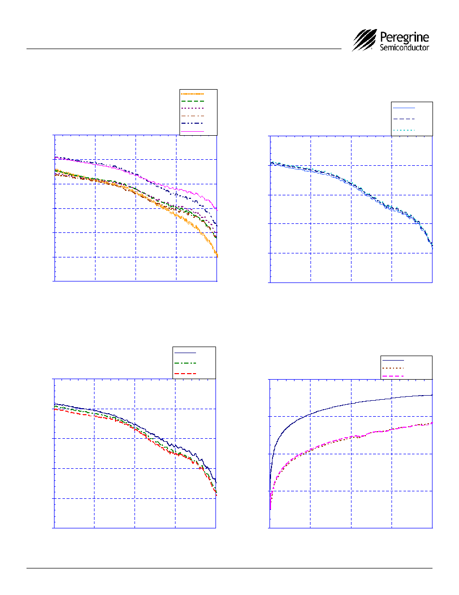
Typical Performance Data @ V
DD
= 2.6 V, 25 ∞C (Unless otherwise noted)
Figure 7. Insertion Loss: TX Over V
DD
Figure 9. Isolation: Worst Case Paths
Figure 8. Insertion Loss: TX Over Temp
Figure 6. Insertion Loss: All Ports
