 | –≠–ª–µ–∫—Ç—Ä–æ–Ω–Ω—ã–π –∫–æ–º–ø–æ–Ω–µ–Ω—Ç: 4273-02 | –°–∫–∞—á–∞—Ç—å:  PDF PDF  ZIP ZIP |
Page 1 of 10
Document No. 70-0174-03
www.psemi.com
©2005 Peregrine Semiconductor Corp. All rights reserved.
Parameter Conditions
Typical
Units
Operation Frequency
1
DC - 3000
MHz
Insertion Loss
1000 MHz
2000 MHz
0.50
0.65
dB
dB
Isolation (RFC - RF1/RF2)
1000 MHz
2000 MHz
34.5
25
dB
dB
Return Loss
1000 MHz
2000 MHz
18.5
14
dB
dB
`ON' Switching Time
3
50% CTRL to 0.1 dB of final value, 1 GHz
0.725
µ
s
`OFF' Switching Time
3
50% CTRL to 25 dB isolation, 1 GHz
0.625
µ
s
Video Feedthrough
2,3
< 2
mV
pp
Input 1 dB Compression
3
1000
MHz
32
dBm
Input IP3
3
1000 MHz, 19 dBm input power
53
dBm
Isolation (RF1 - RF2)
1000 MHz
2000 MHz
40.5
28
dB
dB
Min
DC
32.5
23
38.5
26
30
Max
3000
0.60
0.75
1.5
1.3
RFC
RF1
RF2
CMOS
Control
Driver
V1
V2
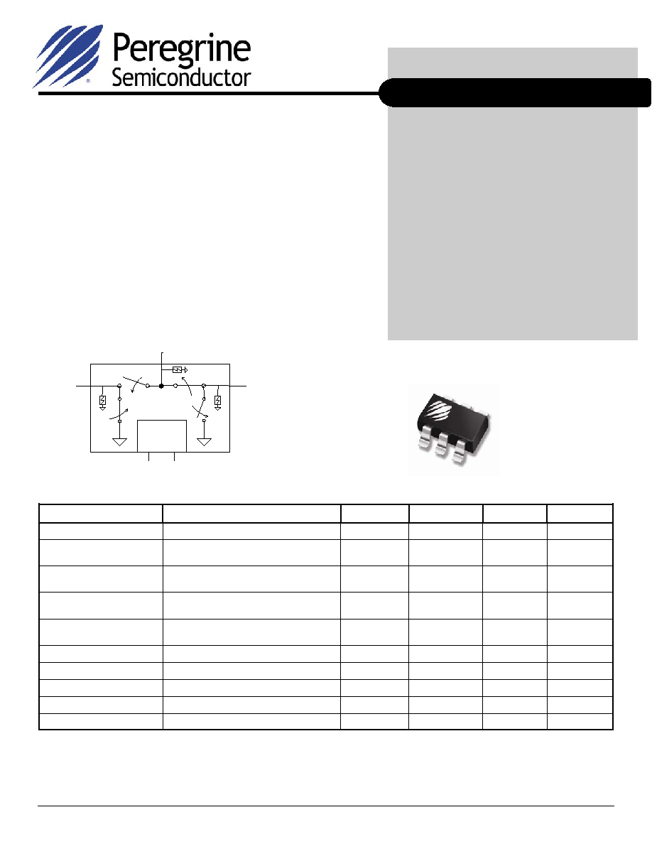
The PE4273 RF Switch is designed for the TV tuner, PCTV, set
top box, DTV, DVR and general broadband applications. This
device offers industry leading broadband linearity, 1.5 kV ESD
tolerance and a simple CMOS interface. It offers a simple
alternative solution to pin diode and mechanical relay switches.
The PE4273 SPDT Broadband RF Switch is manufactured on
Peregrine's UltraCMOSTM process, a patented variation of
silicon-on-insulator (SOI) technology on a sapphire substrate,
offering the performance of GaAs with the economy and
integration of conventional CMOS.
Product Specification
SPDT Broadband UltraCMOSTM
DC ≠ 3 GHz RF Switch
Product Description
Figure 1. Functional Diagram
PE4273
Features
∑
Single-pin or complementary CMOS logic
control inputs
∑
High ESD tolerance of 1.5 kV
∑
Low insertion loss: 0.50 dB at 1000 MHz,
0.65 dB at 2000 MHz
∑
Isolation of 34.5 dB at 1000 MHz, 25 dB at
2000 MHz
∑
Typical input 1 dB compression point of
+32 dBm
∑
Ultra-small SC-70 package
Table 1. Electrical Specifications @ +25 ∞C, V
DD
= 3 V (Z
S
= Z
L
= 75
)
Figure 2. Package Type
6-lead SC-70
Notes:
1. Device linearity will begin to degrade below 10 MHz.
2. Measured with a 1 ns risetime, 0/3 V pulse and 500 MHz bandwidth.
3. Measured in a 50
system.
Product Specification
PE4273
Page 2 of 10
©2005 Peregrine Semiconductor Corp. All rights reserved.
Document No. 70-0174-03
UltraCMOSTM RFIC Solutions
Table 2. Pin Descriptions
Table 3. Absolute Maximum Ratings
Electrostatic Discharge (ESD) Precautions
When handling this UltraCMOSTM device, observe
the same precautions that you would use with
other ESD-sensitive devices. Although this device
contains circuitry to protect it from damage due to
ESD, precautions should be taken to avoid
exceeding the rating specified in Table 3.
Latch-Up Avoidance
Unlike conventional CMOS devices, UltraCMOSTM
devices are immune to latch-up.
Table 4. DC Electrical Specifications
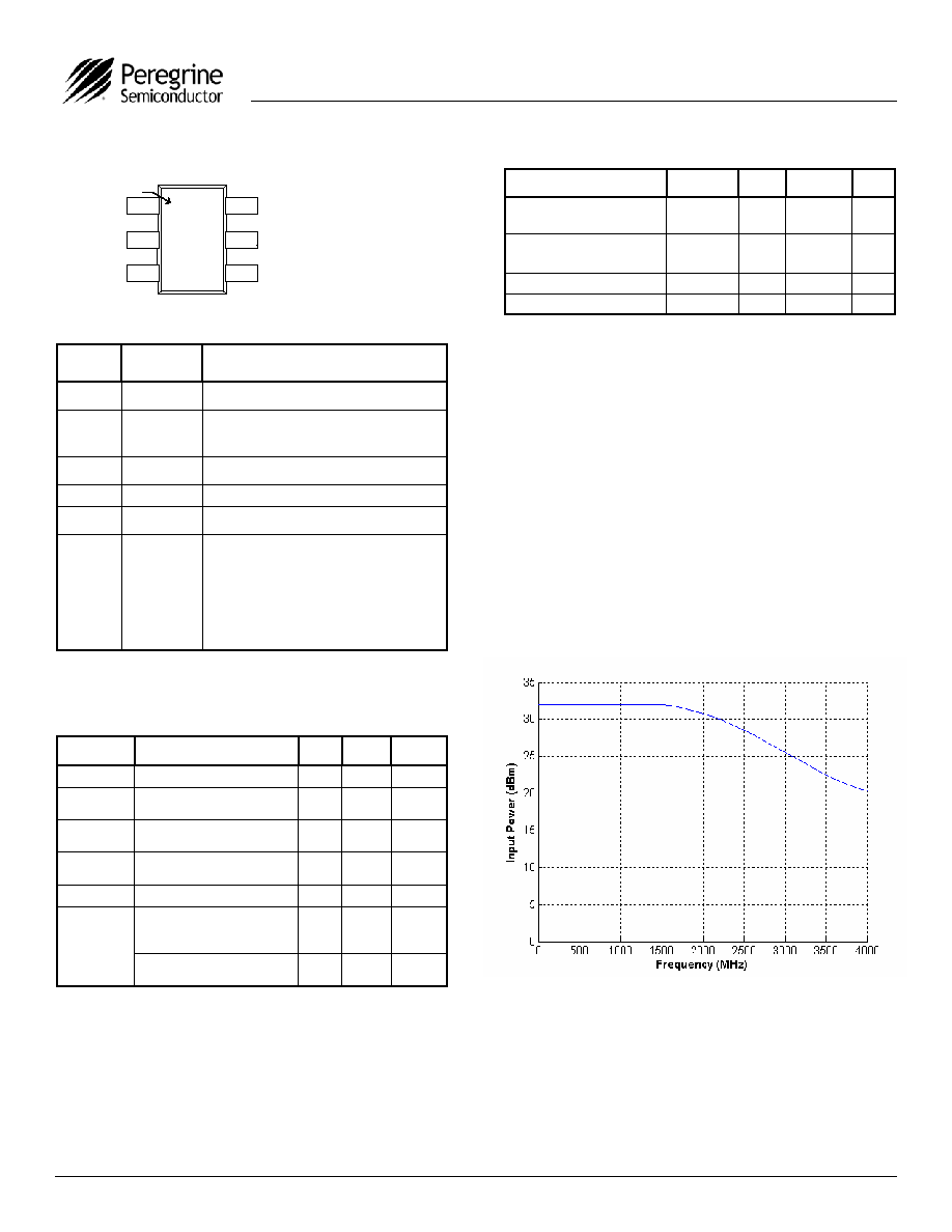
Figure 3. Pin Configuration (Top View)
1
2
3
4
5
6
V2
RFC
V1
RF1
GND
RF2
273
pin 1
Pin
No.
Pin
Name
Description
1 RF1
RF Port1
4
2
GND
Ground connection. Traces should be
physically short and connected to ground
plane for best performance.
3 RF2
RF Port2
4
4
V1
Switch control input, CMOS logic level.
5 RFC
RF Common
4
6
V2
This pin supports two interface options:
Single-pin control mode. A nominal 3-volt
supply connection is required.
Complementary-pin control mode. A
complementary CMOS control signal
to V1 is supplied to this pin.
Symbol Parameter/Conditions Min Max Units
V
DD
Power supply voltage
-0.3
4.0
V
V
I
Voltage on any input
-0.3
V
DD
+
0.3
V
T
ST
Storage temperature
range
-65 150 ∞C
T
OP
Operating temperature
range
-40 85 ∞C
P
IN
Input power (50
)
+34
dBm
V
ESD
ESD Voltage (HBM,
ML_STD 883 Method
3015.7)
1500
V
ESD Voltage (MM,
JEDEC, JESD22-A114-B)
100
V
Parameter Min
Typ
Max
Units
V
DD
Power Supply
Voltage
2.7 3.0 3.3 V
I
DD
Power Supply Current
(V1
= 3V, V2= 3V)
8
50
µA
Control Voltage High
0.7x V
DD
V
Control Voltage Low
0.3x V
DD
V
Note: 4. All RF pins must be DC blocked with an external series
capacitor or held at 0 VDC.
Absolute Maximum Ratings are those values
listed in the above table. Exceeding these values
may cause permanent device damage.
Functional operation should be restricted to the
limits in the DC Electrical Specifications table.
Exposure to absolute maximum ratings for
extended periods may affect device reliability.
Figure 4. Maximum Operating Input Power
5
Note: 5. Operating within DC limits (Table 4).
Product Specification
PE4273
Page 3 of 10
©2005 Peregrine Semiconductor Corp. All rights reserved.
Document No. 70-0174-03
www.psemi.com
Control Voltages
Signal Path
Pin 6 (V2) = V
DD
Pin 4 (V1) = High
RFC to RF1
Pin 6 (V2) = V
DD
Pin 4 (V1) = Low
RFC to RF2
Table 5. Single-pin Control Logic Truth Table
Table 6. Complementary-pin Control Logic
Truth Table
Control Voltages
Signal Path
Pin 6 (V2) = Low
Pin 4 (V1) = High
RFC to RF1
Pin 6 (V2) = High
Pin 4 (V1) = Low
RFC to RF2
Control Logic Input
The PE4273 is a versatile RF CMOS switch that
supports two operating control modes; single-pin
control mode and complementary-pin control
mode.
Single-pin control mode enables the switch to
operate with a single control pin (pin 4) supporting
a +3-volt CMOS logic input, and requires a
dedicated +3-volt power supply connection (pin 6).
This mode of operation reduces the number of
control lines required and simplifies the switch
control interface typically derived from a CMOS
µ
Processor I/O port
.
Complementary-pin control mode allows the
switch to operate using complementary control
pins V1 and V2 (pins 4 & 6), that can be directly
driven by +3-volt CMOS logic or a suitable
µ
Processor I/O port. This enables the PE4273 to
operate in positive control voltage mode within the
PE4273 operating limits.
Product Specification
PE4273
Page 4 of 10
©2005 Peregrine Semiconductor Corp. All rights reserved.
Document No. 70-0174-03
UltraCMOSTM RFIC Solutions
Evaluation Kit
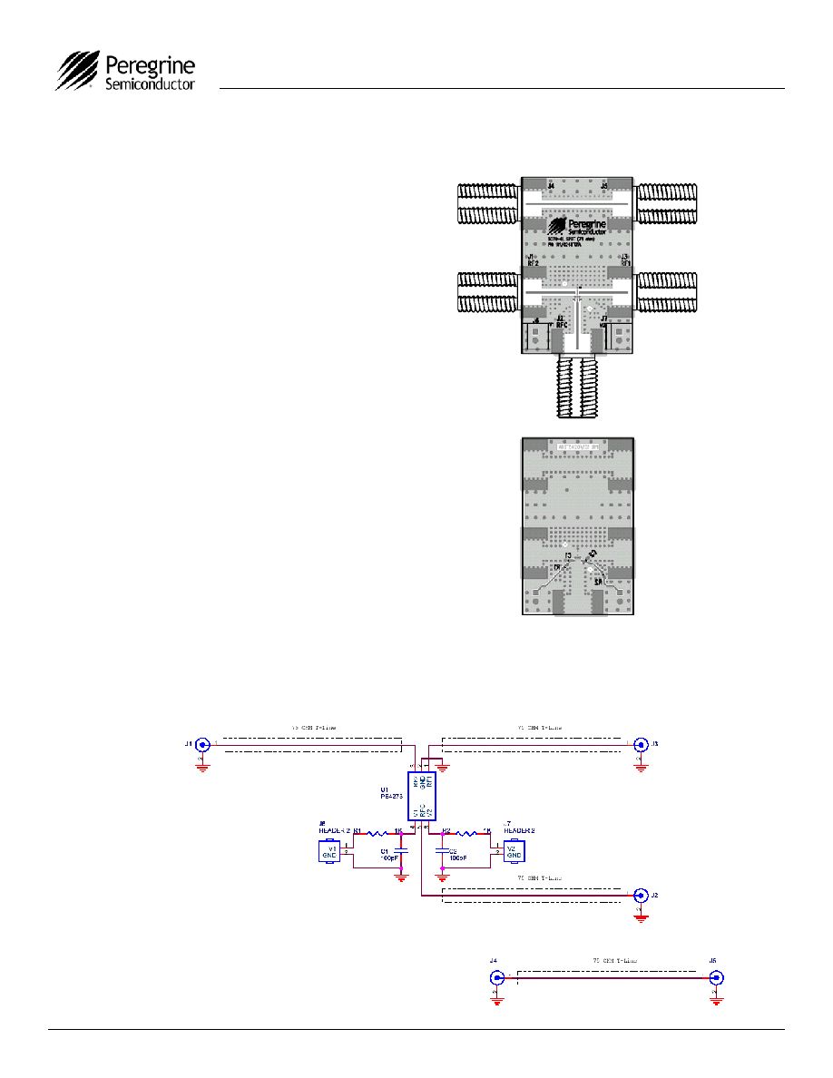
The SPDT Switch Evaluation Kit board was
designed to ease customer evaluation of the
PE4273 SPDT switch. The RF common port is
connected through a 75
transmission line to the
bottom F connector, J2. Port 1 and Port 2 are
connected through 75
transmission lines to two F
connectors on either side of the board, J3 and J1. A
through transmission line connects F connectors J4
and J5. This transmission line can be used to
estimate the loss of the PCB over the environmental
conditions being evaluated.
The board is constructed of a two metal layer FR4
material with a total thickness of 0.031". The bottom
layer provides ground for the RF transmission lines.
The transmission lines were designed using a
coplanar waveguide with ground plane model using
a trace width of 0.021", trace gaps of 0.030",
dielectric thickness of 0.028", copper thickness of
0.0021" and
r
of 4.3.
J6 and J7 provide a means for controlling the DC
inputs to the device. The lower left header (J6) is
connected to the device V1 input. The lower right
header (J7) is connected to the device V2
input.
Series resistors (R1 and R2) are provided to reduce
the package resonance between RF and DC lines.
Footprints for decoupling capacitors (100 pF) are
provided on both V1 and V2 traces. It is the
responsibility of the customer to determine proper
supply decoupling for their design application.
Removing these components from the evaluation
board has not been shown to degrade RF
performance.
Figure 5. Evaluation Board Layouts
Figure 6. Evaluation Board Schematic
Peregrine Specification 102/0311
Peregrine Specification 101/0245
Product Specification
PE4273
Page 5 of 10
©2005 Peregrine Semiconductor Corp. All rights reserved.
Document No. 70-0174-03
www.psemi.com
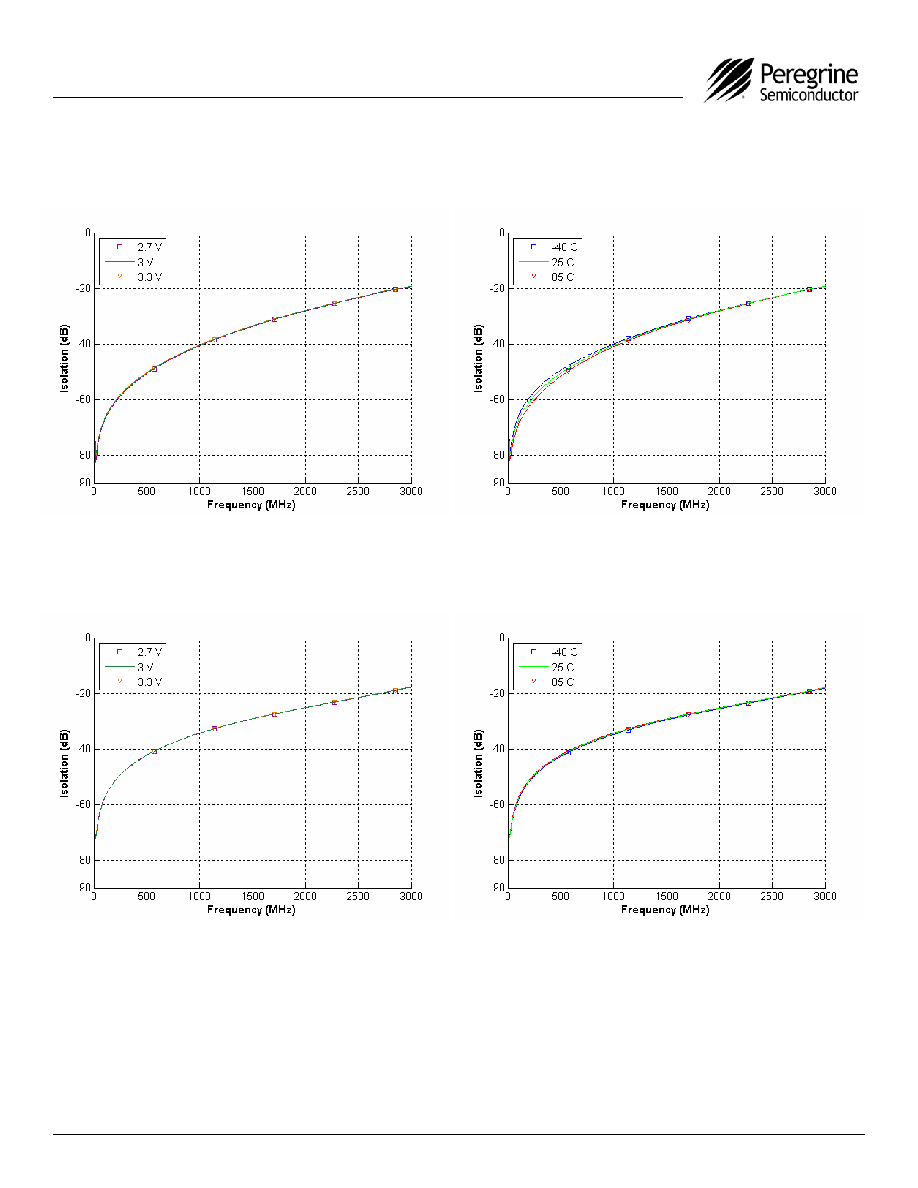
Typical Performance Data
Figure 8. Isolation: RF1 - RF2 @ 3.0 V
Figure 10. Isolation: RFC - RF1/RF2 @ 3.0 V
Figure 7. Isolation: RF1 - RF2 @ 25 ∞C
Figure 9. Isolation: RFC - RF1/RF2 @ 25 ∞C