 | –≠–ª–µ–∫—Ç—Ä–æ–Ω–Ω—ã–π –∫–æ–º–ø–æ–Ω–µ–Ω—Ç: 4274-51 | –°–∫–∞—á–∞—Ç—å:  PDF PDF  ZIP ZIP |

Peregrine Semiconductor Corp. Æ
http://www.psemi.com
Copyright © Peregrine Semiconductor Corp. 2005
Page 1 of 12
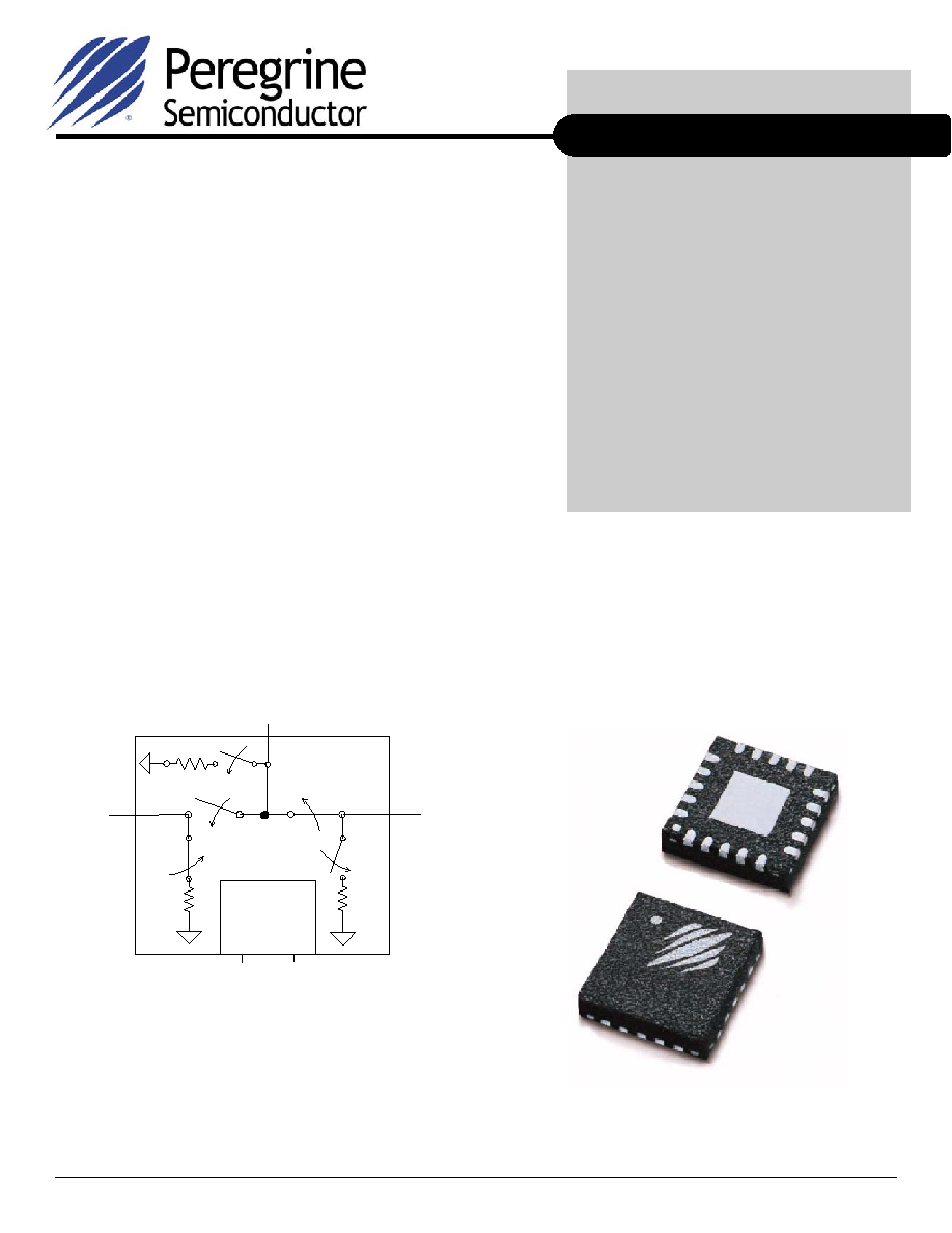
4x4mm 20 pin QFN
RFCommon
RF1
RF2
CTRL1
75
75
75
CTRL2
CMOS
Control
Driver
The PE4274 is an SPDT
UltraCMOSTM
Switch designed for
Broadband applications such as CATV, DTV, Multi-Tuner
DVR (Digital Video Recorder), Set-top Box, PCTV and
Game Boxes. It offers high isolation and low insertion loss
in both a powered and a unique unpowered default state.
The PE4274 covers a broad frequency range from near DC
to beyond 2.2 GHz with a single positive supply and CMOS
control. The PE4274 provides a smaller, cost effective,
more reliable and manufacturable alternative to mechanical
relays in some set-top box applications.
The PE4274 is manufactured in Peregrine's patented Ultra
Thin Silicon (UTSiÆ) CMOS process, offering the
performance of GaAs with the economy and integration of
conventional CMOS.
Preliminary Specification
Product Description
Figure 1. Functional Diagram
PE4274
Features
∑
Unpowered operational state
∑
All-Off terminated state
∑
CTB performance of 90dBc
∑
High isolation 63 dB at 1 GHz
∑
Low insertion loss: typically 0.5 dB at
5 MHz, 0.8 dB at 1 GHz
∑
CMOS two-pin control
∑
Single +3 volt supply operation
∑
1 kV ESD
∑
Low current consumption: 8
µ
A
75
Terminated - 2.2 GHz SPDT
CATV UltraCMOSTM Switch
Featuring - Unpowered Operation
Figure 2. Package Type

Preliminary Specification
Copyright © Peregrine Semiconductor Corp. 2005
File No. 70/0185-01A
UltraCMOSTM RFIC Solutions
PE4274
Page 2 of 12
Parameter Condition
Minimum
Typical
Maximum
Units
Operating Frequency
1
5
2200
MHz
RF1-RFC Insertion Loss
(Powered / Unpowered)
5 MHz ≠ 216 MHz
216 MHz ≠ 550 MHz
550 MHz ≠ 806 MHz
806 MHz ≠ 2200 MHz
0.5 / 1.5
0.5 / 1.5
0.8 / 1.8
1.0 / 2.2
dB
RF2-RFC Insertion Loss
5 MHz ≠ 216 MHz
216 MHz ≠ 550 MHz
550 MHz ≠ 806 MHz
806 MHz ≠ 2200 MHz
0.7
0.8
1.0
1.3
dB
Isolation RF1 or RF2 to RFC
(Powered /RF2 Unpowered)
5 MHz ≠ 216 MHz
216 MHz ≠ 550 MHz
550 MHz ≠ 806 MHz
806 MHz ≠ 2200 MHz
97 / 95
84 / 80
69 / 69
57 / 56
dB
Isolation RF1 to RF2
2
5 MHz ≠ 216 MHz
216 MHz ≠ 550 MHz
550 MHz ≠ 806 MHz
806 MHz ≠ 2200 MHz
80 / 82
70 / 71
63 / 65
61 / 65
dB
Input IP2
3
(Powered/Unpowered)
5 MHz - 1000 MHz
90 / 73
dBm
Input IP3
3
(Powered/Unpowered)
5 MHz - 1000 MHz
50 / 39
dBm
Input 1dB Compression
3
(Powered/Unpowered)
1000 MHz
30 / 24
dBm
CTB / CSO
(Powered/Unpowered)
77 & 110 channels;
Power Out = 44 dBmV
-90 / -77
dBc
Switching Time
50% CTRL to 10 / 90 RF
2
µs
Video Feedthrough
4
5 MHz - 1000 MHz
15
mV
pp
Table 1. Electrical Specifications @ +25 ∞C, V
DD
= +3 V (Z
S
= Z
L
= 75
)
Notes: 1. Device linearity will begin to degrade with input signals below 5 MHz.
2. Isolation at 216 MHz = 75 dB
3. Measured in a 50 system.
4. Measured with a 1 ns risetime, 0/3 V pulse and 500 MHz bandwidth

Preliminary Specification
Peregrine Semiconductor Corp. Æ
http://www.psemi.com
Copyright © Peregrine Semiconductor Corp. 2005
PE4274
Page 3 of 12
GND
15
14
13
12
11
3
4
5
2
1
17
16
18
19
20
9
10
8
7
6
C2
GND
GND
GND
GND
GND
RF
C
VD
D
C1
VSS
/
G
N
D
GND
GND
GND
RF2
GND, RF2 Term.
GND
GND, RF1 Term.
RF1
GND
GND
75
75
150
150
No.
Name
Description
1
GND
RF Ground
2
GND
RF Ground
3
1
RF1
RF I/O
4
GND
RF Ground, RF1 Termination Resistor
5
GND
RF Ground
6
GND
RF Ground
7
GND
RF Ground
8
1
RFC
RF Common
9
GND
RF Ground
10
GND
RF Ground
11
GND
RF Ground
12
GND
RF Ground, RF2 Termination Resistor
13
1
RF2
RF I/O
14
GND
RF Ground
15
GND
RF Ground
16
2
C2
Control 2
17
2
C1
Control 1
18
3
VSS / GND
Negative Supply Option
19
GND
Digital Ground
20
VDD
Supply
Pad
GND
RF Ground Pad
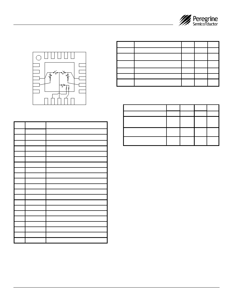
Table 2. Pin Descriptions
Table 3. Absolute Maximum Ratings
Electrostatic Discharge (ESD) Precautions
When handling this UltraCMOSTM device, observe
the same precautions that you would use with
other ESD-sensitive devices. Although this device
contains circuitry to protect it from damage due to
ESD, precautions should be taken to avoid
exceeding the rating specified.
Latch-Up Avoidance
Unlike conventional CMOS devices, UltraCMOSTM
devices are immune to latch-up.
Table 4. DC Electrical Specifications @ 25 ∞C
Notes:
1. RF pins 3, 8, and 13 must be at 0 VDC. The RF pins do not
require DC blocking capacitors for proper operation if the 0 V DC
requirement is met.
2. Pins 16 and 17 are the CMOS controls that set the four operating
states.
3. Connect pin 18 to GND to enable the negative voltage generator.
Connect
pin 18 to V
SS
(-3V) to bypass and disable internal -3V supply
generator. See "Switching Frequency".
Switching Frequency
The PE4274 has a maximum 25 kHz switching
rate when the internal negative voltage generator
is used (pin 18 = GND). The rate at which the
PE4274 can be switched is only limited to the
switching time if an external -3 V supply is
provided at (pin 18 = V
SS
).
Figure 3. Pin Configuration (Top View)
4x4mm 20-Lead QFN
Symbol Parameter/Condition Min
Max
Unit
V
DD
Power supply voltage
-0.3
4.0
V
V
I
Voltage on CTRL input
-0.3
V
DD
+
0.3
V
P
RF
RF power on RFC, RF1, RF2
Terminated/Through
24/33
dBm
T
ST
Storage temperature
-65
+150
∞C
T
OP
Operating temperature
-40
+85
∞C
V
ESD
ESD voltage
(Human Body Model)
1,000
V
Parameter Min
Typ
Max
Unit
V
DD
Power Supply
2.7
3.0
3.3
V
I
DD
Power Supply Current
(V
DD
= 3 V, V
CNTL
= 3 V)
8
µA
Control Voltage High
0.7 x
V
DD
V
DD
V
Control Voltage Low
0
0.3 x
V
DD
V

Preliminary Specification
Copyright © Peregrine Semiconductor Corp. 2005
File No. 70/0185-01A
UltraCMOSTM RFIC Solutions
PE4274
Page 4 of 12
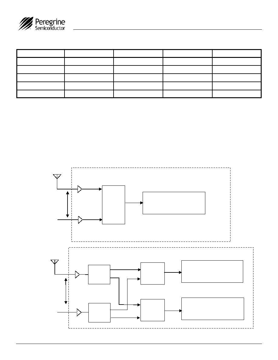
Figure 4. Typical Application Block Diagram
Table 5. Truth Table
V
DD
C1
C2
RFC ≠ RF1
RFC ≠ RF2
OFF
Low
Low
ON
OFF
ON
Low
Low
OFF
OFF
ON
Low
High
OFF
ON
ON
High
Low
ON
OFF
ON
High
High
N/A
1
N/A
1
Notes:
1. The operation of the PE4274 is not supported or characterized in the C1 = High and C2 =
High state.
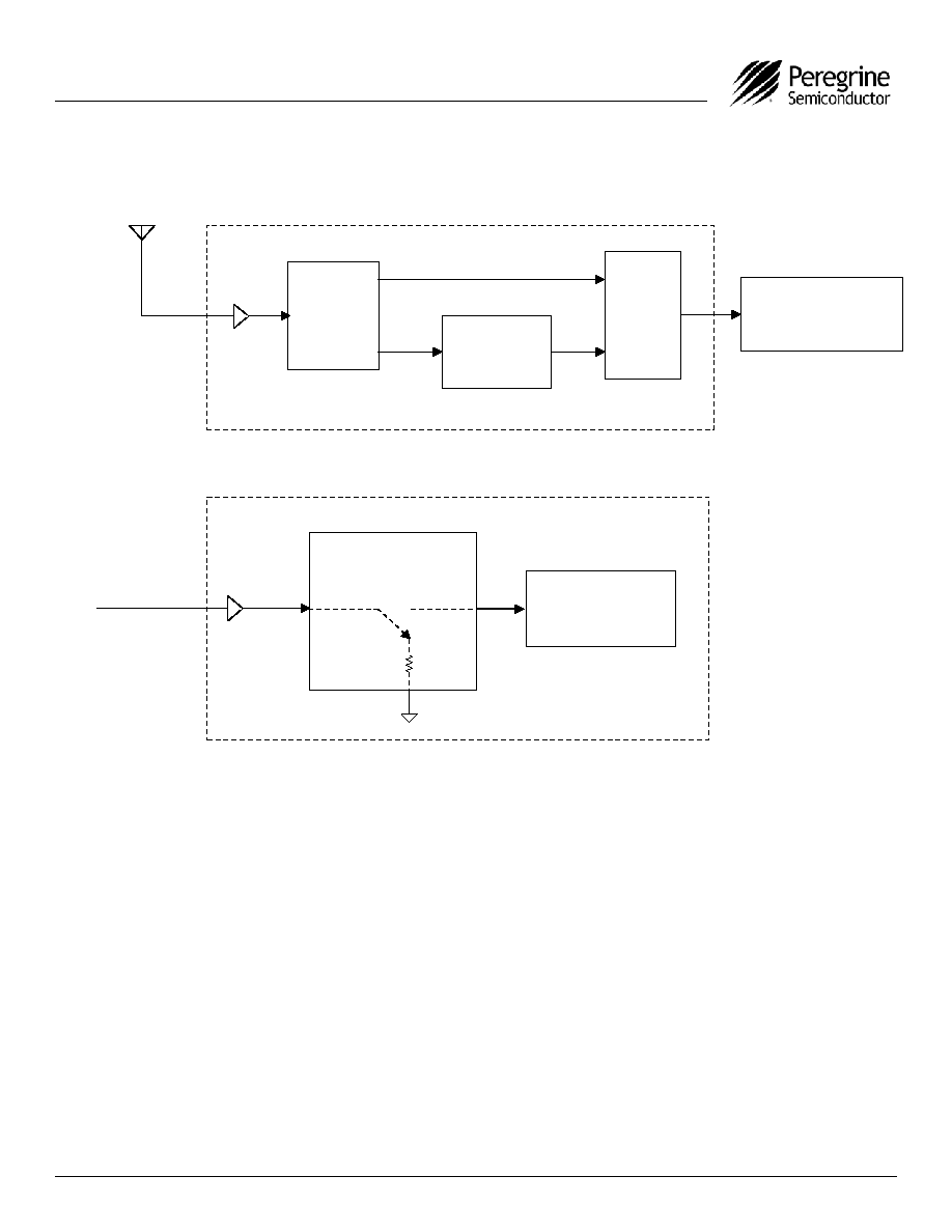
The PE4274 provides the high isolation
required by FCC part 15.115 regulation
between the television antenna and the cable
plant. The advantage of the PE4274 is that
device isolation / thru performance is
maintained when power is removed. This
unique feature makes the PE4274 ideal for set-top
box and VCR applications.
The PE4274 supports signal flow from RFC to
RF1 and RF2 termination in the unpowered state;
similar to the powered state with C1=High,
C2=Low.
DTV-Tuner
PE4274
SPDT
Antenna Input
CATV Input
80dB 54 ≠ 216MHz
60dB 216 ≠ 550MHz
55dB 550 ≠ 806MHz
DTV-Tuner
PE4274
SPDT
DTV Tuner
Antenna Input
CATV Input
80dB 54 ≠ 216MHz
60dB 216 ≠ 550MHz
55dB 550 ≠ 806MHz
Power
Splitter
Power
Splitter
PE4274
SPDT
Dual Tuner DTV / DVR / Set-top Box

Preliminary Specification
Peregrine Semiconductor Corp. Æ
http://www.psemi.com
Copyright © Peregrine Semiconductor Corp. 2005
PE4274
Page 5 of 12
Television
RF
Splitter
Antenna/Cable
Input
PVR/VCR/Game Box
PE4274
SPDT
Tuner/
Modulator
OFF ≠ Pass Through
Tuner
CATV Input
OFF ≠ Terminated
TV Set / Cable Set-top Box
75W
PE4274 SPDT
RF1
RF2
RF2
