Page 1 of 11
Document No. 70/0056~02D
www.psemi.com
©2005 Peregrine Semiconductor Corp. All rights reserved.
4x4mm -20 Lead QFN
The PE4302 is a high linearity, 6-bit RF Digital Step Attenuator
"DSA" covering a 31.5 dB attenuation range in 0.5 dB steps.
This 50-ohm RF DSA provides both parallel and serial CMOS
control interface operates on a single 3-volt supply and
maintains high attenuation accuracy over frequency and
temperature. It also has a unique control interface that allows
the user to select an initial attenuation state at power-up. The
PE4302 exhibits very low insertion loss and low power
consumption. This functionality is delivered in a 4x4mm QFN
footprint.
The PE4302 is manufactured in Peregrine's patented Ultra
Thin Silicon (UTSiÆ) CMOS process, offering the performance
of GaAs with the economy and integration of conventional
CMOS
.
Product Specification
50
RF Digital Attenuator
6-bit, 31.5 dB, DC ≠ 4.0 GHz
Product Description
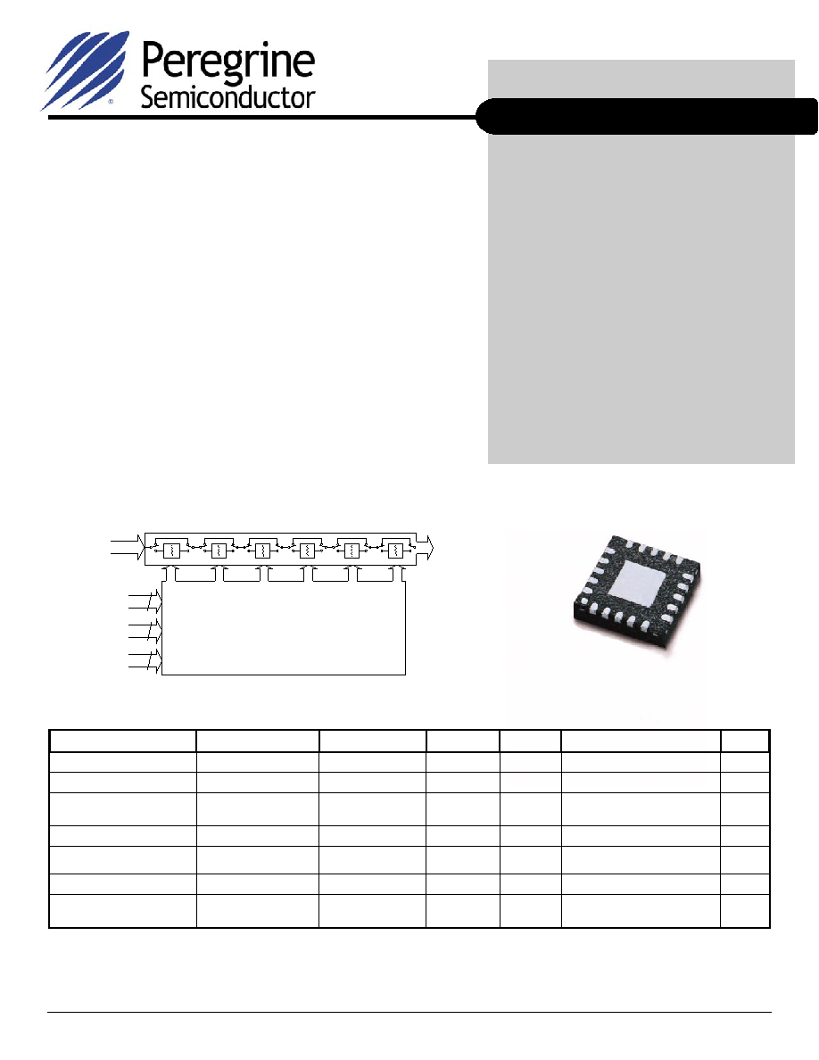
Figure 1. Functional Schematic Diagram
PE4302
Features
∑
Attenuation: 0.5 dB steps to 31.5 dB
∑
Flexible parallel and serial programming
interfaces
∑
Unique power-up state selection
∑
Positive CMOS control logic
∑
High attenuation accuracy and linearity
over temperature and frequency
∑
Very low power consumption
∑
Single-supply operation
∑
50
impedance
∑
Packaged in a 20 lead 4x4mm QFN
Control Logic Interface
Parallel Control
Power-Up Control
Serial Control
RF Input
RF Output
Switched Attenuator Array
6
3
2
Figure 2. Package Type
Table 1. Electrical Specifications @ +25∞C, V
DD
= 3.0 V
Parameter Test
Conditions
Frequency
Minimum
Typical Maximum Units
Operation Frequency
DC
4000
MHz
Insertion Loss
2
DC - 2.2 GHz
-
1.5
1.75
dB
Attenuation Accuracy
Any Bit or Bit
Combination
DC
1.0 GHz
1.0 < 2.2 GHz
- -
±(0.10 + 3% of atten setting)
±(0.15 + 5% of atten setting)
dB
dB
1 dB Compression
3
1 MHz - 2.2 GHz
30
34
-
dBm
Input IP3
1,2
Two-tone inputs
+18 dBm
1 MHz - 2.2 GHz
-
52
-
dBm
Return Loss
DC - 2.2 GHz
15
20
- dB
Switching Speed
50% control to 0.5 dB
of final value
-
- 1
µ
s
Notes: 1. Device Linearity will begin to degrade below 1 Mhz
2. See Max input rating in Table 2 & Figures on Pages 2 to 4 for data across frequency.
3. Note Absolute Maximum in Table 3.

Product Specification
PE4302
Page 5 of 11
Document No. 70/0056~02D
www.psemi.com
©2005 Peregrine Semiconductor Corp. All rights reserved.
Table 2. Pin Descriptions
Table 3. Absolute Maximum Ratings
Electrostatic Discharge (ESD) Precautions
When handling this UltraCMOSTM device, observe
the same precautions that you would use with
other ESD-sensitive devices. Although this device
contains circuitry to protect it from damage due to
ESD, precautions should be taken to avoid
exceeding the rate specified in Table 3.
Exposed Solder Pad Connection
The exposed solder pad on the bottom of the
package must be grounded for proper device
operation.
Table 4. DC Electrical Specifications
Note 1: Both RF ports must be held at 0 V
DC
or DC blocked with an
external series capacitor.
2: Latch Enable (LE) has an internal 100 k resistor to V
DD.
3: Connect pin 12 to GND to enable internal negative voltage
generator. Connect pin 12 to V
SS
(-VDD) to bypass and
disable internal negative voltage generator.
4. Place a 10 k resistor in series, as close to pin as possible
to avoid frequency resonance.
Figure 14. Pin Configuration (Top View)
V
DD
PU
P1
PU
P2
V
DD
GND
1
20
19
18
17
16
15
14
13
12
11
6
7
8
9
10
2
3
4
5
C16
RF1
Data
Clock
LE
GND
Vss/GND
P/S
RF2
C8
C4
C2
GN
D
C1
C0
.
5
20-lead QFN
4x4mm
Exposed Solder Pad
Pin
No.
Pin
Name
Description
1
C16
Attenuation control bit, 16dB (Note 4).
2
RF1
RF port (Note 1).
3
Data
Serial interface data input (Note 4).
4
Clock
Serial interface clock input.
5
LE
Latch Enable input (Note 2).
6 V
DD
Power supply pin.
7
PUP1
Power-up selection bit, MSB.
8
PUP2
Power-up selection bit, LSB.
9 V
DD
Power supply pin.
10 GND
Ground
connection.
11 GND
Ground
connection.
12 V
ss
/GND
Negative supply voltage or GND
connection(Note 3)
13
P/S
Parallel/Serial mode select.
14
RF2
RF port (Note 1).
15
C8
Attenuation control bit, 8 dB.
16
C4
Attenuation control bit, 4 dB.
17
C2
Attenuation control bit, 2 dB.
18 GND
Ground
connection.
19
C1
Attenuation control bit, 1 dB.
20
C0.5
Attenuation control bit, 0.5 dB.
Paddle
GND
Ground for proper operation
Symbol Parameter/Conditions Min Max Units
V
DD
Power
supply
voltage
-0.3
4.0 V
V
I
Voltage on any input
-0.3
V
DD
+
0.3
V
T
ST
Storage temperature range
-65
150
∞C
T
OP
Operating temperature
range
-40 85 ∞C
P
IN
Input power (50
)
24
dBm
V
ESD
ESD voltage (Human Body
Model)
500
V
Parameter Min
Typ
Max
Units
V
DD
Power Supply
Voltage
2.7 3.0 3.3 V
I
DD
Power Supply
Current
100
µ
A
Digital Input High
0.7xV
DD
V
Digital Input Low
0.3xV
DD
V
Digital Input Leakage
1
µ
A
Latch-Up Avoidance
Unlike conventional CMOS devices, UltraCMOSTM
devices are immune to latch-up.
Switching Frequency
The PE4302 has a maximum 25kHz switching
rate.
Resistor on Pin 1 & 3
A 10 k
resistor on the inputs to Pin 1 & 3 (see
Figure 16) will eliminate package resonance
between the RF input pin and the two digital
inputs. Specified attenuation error versus
frequency performance is dependent upon this
condition.