 | –≠–ª–µ–∫—Ç—Ä–æ–Ω–Ω—ã–π –∫–æ–º–ø–æ–Ω–µ–Ω—Ç: 83501-00 | –°–∫–∞—á–∞—Ç—å:  PDF PDF  ZIP ZIP |
PEREGRINE SEMICONDUCTOR CORP.
|
http://www.peregrine-semi.com
Copyright
Peregrine Semiconductor Corp. 2003
Page 1 of 7
Product Description
Military Operating Temperature Range
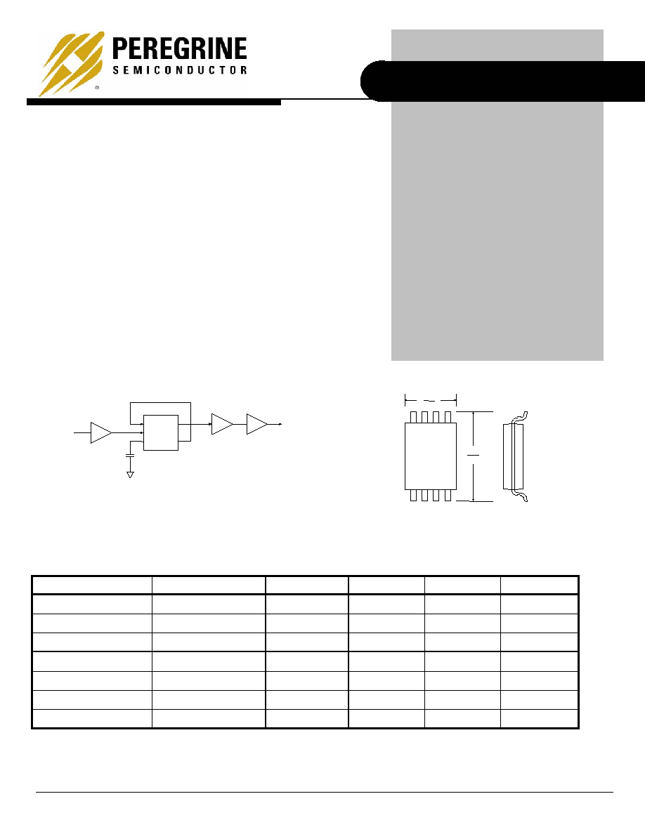
Figure 1. Functional Schematic Diagram
Figure 2. Package Drawing
Table 1. Electrical Specifications
(Z
S
= Z
L
= 50
)
2.85V V
DD
3.15 V; -55
∞ C T
A
125
∞ C,
unless otherwise specified
Parameter Conditions
Minimum
Typical
Maximum
Units
Supply Voltage
2.85
3.0
3.15
V
Supply Current
13
18
mA
Input Frequency (F
in
)
400
3500
MHz
Input Power (P
in
) 400
MHz
F
in
2.0 GHz
-10
+10
dBm
2.0 GHz < F
in
2.8 GHz
0
+10
dBm
2.8 GHz < F
in
3.5 GHz
+5
+10
dBm
Output Power (P
out
) 400
MHz
F
in
3.5 GHz
-15
dBm
PRODUCT SPECIFICATION
PE83501
Military Operating Temperature Range
3.5 GHz Low Power CMOS
Divide-by-2 Prescaler
Features
∑ High-frequency operation:
400 MHz to 3.5 GHz
∑ Fixed divide ratio of 2
∑ Low-power operation: 12 mA
typical @ 3 V
∑ Small package: 8-lead MSOP
∑ Low cost
The PE83501 is a high-performance dynamic CMOS
prescaler with a fixed divide ratio of 2. Its operating
frequency range is 400 MHz to 3.5 GHz. The PE83501
operates on a nominal 3 V supply and draws only 12 mA.
It is packaged in a small 8-lead MSOP and is ideal for
frequency scaling and microwave PLL synthesis
solutions.
The PE83501 is manufactured in Peregrine's patented
Ultra-Thin Silicon (UTSi
) CMOS process, offering the
performance of GaAs with the economy and integration
of conventional CMOS.
5.05
4.75
8-lead MSOP
3.05
2.85
PREAMP
DRIVER
OUTPUT BUFFER
D Q
CLK
DEC QB
OFF-CHIP
BYPASS
F
in
F
out
PE83501
Product Specification
Copyright
Peregrine Semiconductor Corp. 2003
File No. 70/0124~00B
|
UTSi
CMOS RFIC SOLUTIONS
Page 2 of 7
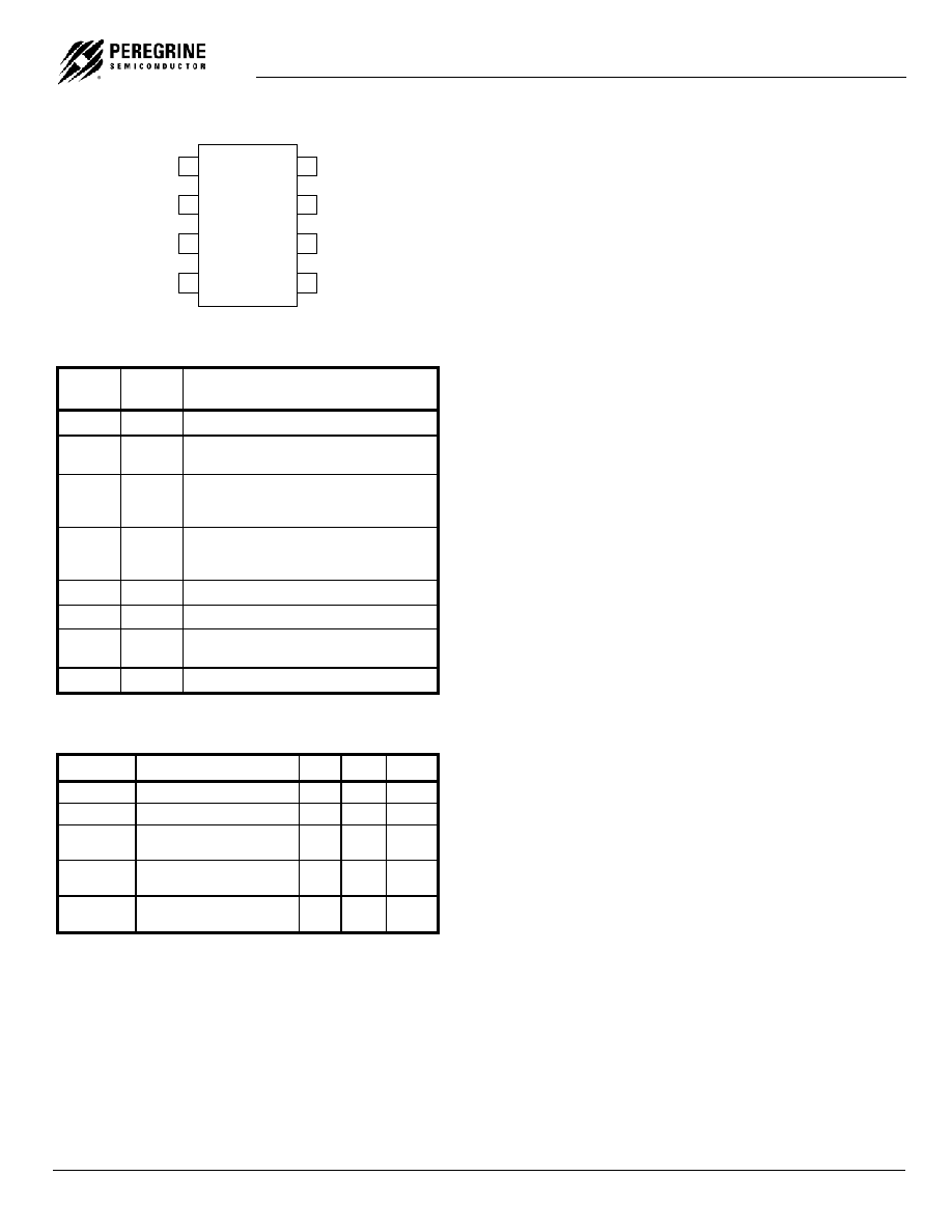
Figure 3. Pin Configuration
Table 2. Pin Descriptions
Pin
No.
Pin
Name
Description
1
VDD
Power supply pin. Bypassing is required.
2 F
in
Input signal pin. DC blocking capacitor
required (15 pF typical)
3 DEC
Power supply decoupling pin. Place a
capacitor as close as possible and connect
directly to the ground plane.
4 GND
Ground pin. Ground pattern on the board
should be as wide as possible to reduce
ground impedance.
5 GND
Ground
pin.
6 GND
Ground
pin.
7 F
out
Divided frequency output pin. DC blocking
capacitor required (47 pF typical)
8 GND
Ground
pin.
Table 3. Absolute Maximum Ratings
Symbol Parameter/Conditions Min Max Units
VDD Supply
voltage
4.0 V
P
in
Input
Power
15
dBm
T
ST
Storage
temperature
range
-65 150
∞C
T
OP
Operating
temperature
range
-55 125
∞C
VESD
ESD voltage (Human
Body Model)
250 V
Electrostatic Discharge (ESD) Precautions
When handling this UTSi device, observe the same
precautions that you would use with other ESD-
sensitive devices. Although this device contains
circuitry to protect it from damage due to ESD,
precautions should be taken to avoid exceeding the
rating specified in Table 3.
Latch-Up Avoidance
Unlike conventional CMOS devices, UTSi CMOS
devices are immune to latch-up.
Device Functional Considerations
The PE83501 divides a 400 MHz to 3.5 GHz input
signal by two, producing a 200 MHz to 1.75 GHz
output signal. To work properly, pin 3 must be
supplied with a bypass capacitor to ground. In
addition, the input and output signals (pins 2 & 7)
must be AC coupled via an external capacitor, as
shown in the test circuit in Figure 4.
The ground pattern on the board should be made
as wide as possible to minimize ground
impedance. See Figure 11 for a layout example.
PE83501
1
2
3
4
8
7
6
5
F
in
GND
DEC
GND
F
out
VDD
GND
GND
PE83501
Product Specification
PEREGRINE SEMICONDUCTOR CORP.
|
http://www.peregrine-semi.com
Copyright
Peregrine Semiconductor Corp. 2003
Page 3 of 7
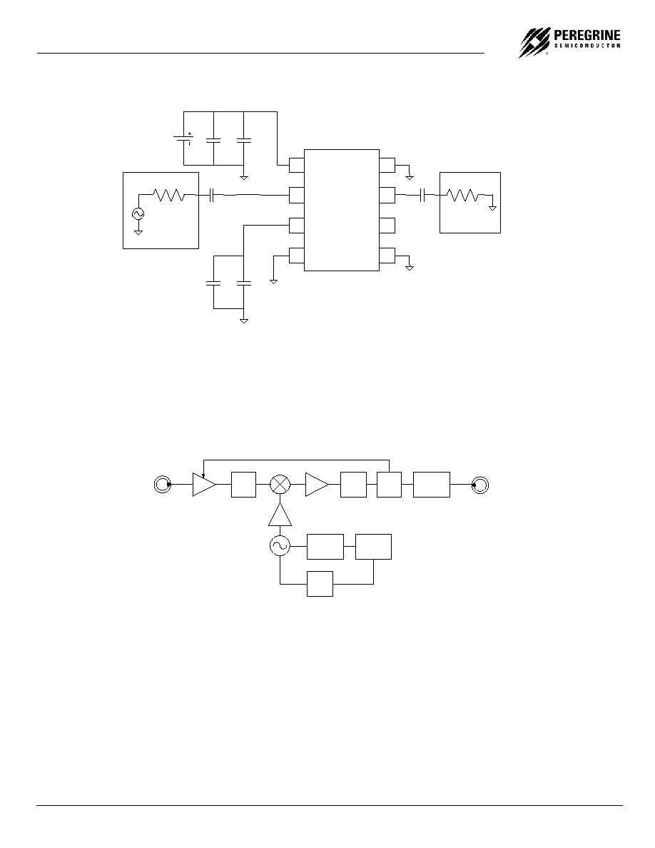
Figure 4. Test Circuit Block Diagram
Figure 5. High Frequency System Application
The wideband frequency of operation of the PE83501 makes it an ideal part for use in a DBS downconverter
system.
Signal Generator
Spectrum
Analyzer
PE83501
1
2
3
4
8
7
6
5
10 pF
15 pF
50
VDD
3 V +/
-
0.15 V
1000 pF
47 pF
10 pF
10 nF
50
N/C
BPF
SAW
AGC
FM
DEMOD
PE83501
PE3236
LOW NOISE
PLL SYNTH
LPF
INPUT FROM
DBS 1
ST
IF
BASEBAND
OUTPUT
DIVIDE-BY-2
8 Lead
MSOP

PE83501
Product Specification
Copyright
Peregrine Semiconductor Corp. 2003
File No. 70/0124~00B
|
UTSi
CMOS RFIC SOLUTIONS
Page 4 of 7
Typical Performance Data: V
DD
= 3.0V
Figure 6. Input Sensitivity
Figure 7. Device Current
Figure 8. Output Power
PE83501
Product Specification
PEREGRINE SEMICONDUCTOR CORP.
|
http://www.peregrine-semi.com
Copyright
Peregrine Semiconductor Corp. 2003
Page 5 of 7
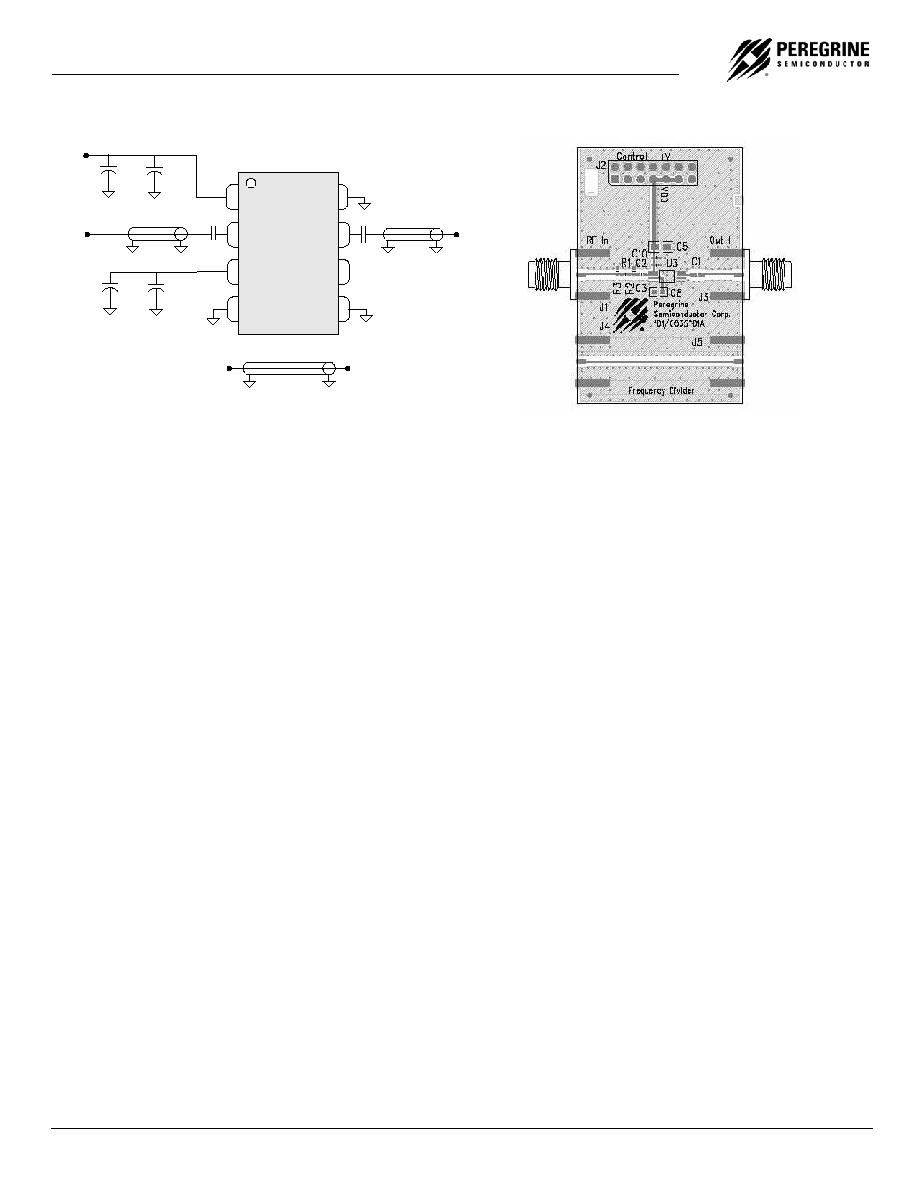
VDD
IN
DEC
GND
GND
OUT
NC
GND
1000 pF
J2-7
J3
J4
J5
10 pF
C1
J1
10 pF
10 nF
C2
Figure 10. Evaluation Board Schematic Diagram
Figure 11. Evaluation Board Layout
Evaluation Kit Operation
The MSOP Prescaler Evaluation Board was
designed to help customers evaluate the PE83501
Divide-by-2 Prescaler. On this board, the device
input (pin 2) is connected to connector J1 through a
50 transmission line. A series capacitor (C3)
provides the necessary DC block for the device
input. It is important to note that the value of this
capacitance will impact the performance of the
device. A value of 15 pF was found to be optimal
for this board layout; other applications may require
a different value.
The device output (pin 7) is connected to connector
J3 through a 50 transmission line. A series
capacitor (C1) provides the necessary DC block for
the device output. Note that this capacitor must be
chosen to have a low impedance at the desired
output frequency the device. The value of 47 pF
was chosen to provide a wide operating range for
the evaluation board.
The board is constructed of a two-layer FR4
material with a total thickness of 0.031". The
bottom layer provides ground for the RF
transmission lines. The transmission lines were
designed using a coplanar waveguide above
ground plane model with trace width of 0.030", trace
gaps of 0.007", dielectric thickness of 0.028", metal
thickness of 0.0014" and
r
of 4.4. Note that the
predominate mode for these transmission lines is
coplanar waveguide.
J2 provides DC power to the device. Starting from
the lower left pin, the second pin to the right (J2-3)
is connected to the device VDD pin (1). Two
decoupling capacitors (10 pF, 1000 pF) are
included on this trace. It is the responsibility of the
customer to determine proper supply decoupling for
their design application.
The DEC pin (3) must be connected to a low
impedance AC ground for proper device operation.
On the board, two decoupling capacitors (C6 = 10
nF, C4 = 10 pF), located on the back of the board,
perform this function.
Applications Support
If you have a problem with your evaluation kit or if
you have applications questions call (858) 455-0660
and ask for applications support. You may also
contact us by fax or e-mail:
Fax: (858) 455-0770
E-Mail: help@peregrine-semi.com
C3
C1

PE83501
Product Specification
Copyright
Peregrine Semiconductor Corp. 2003
File No. 70/0124~00B
|
UTSi
CMOS RFIC SOLUTIONS
Page 6 of 7
FRONT VIEW
2.95±0.10
0.08
A B C
0.33+0.07
-0.08
0.10 A
0.10±0.05
3.00±0.10
0.86±0.08
1.10 MAX
- C -
- A -
1
0.65BSC
0.51±0.13
2.45±0.10
0.51±0.13
2X
8
3.00±0.10
.25 A B C
2
3
4
- B -
.525BSC
TOP VIEW
5
6
7
4.90±0.15
3.00±0.10
SIDE VIEW
2.95±0.10
Figure 10. Package Drawing
8-Lead MSOP
Table 6. Ordering Information
Order
Code
Part Marking
Description
Package
Shipping
Method
83501-11
PE83501
PE83501-08MSOP-100A
8-lead MSOP
50 pcs. / Tube
83501-12
PE83501
PE83501-08MSOP-2000C
8-lead MSOP
2000 pcs. / T&R
83501-00
PE83501-EK
PE83501-08MSOP-EK
Evaluation Board
1 / Box

PE83501
Product Specification
PEREGRINE SEMICONDUCTOR CORP.
|
http://www.peregrine-semi.com
Copyright
Peregrine Semiconductor Corp. 2003
Page 7 of 7
Sales Offices
United States
Peregrine Semiconductor Corp.
6175 Nancy Ridge Drive
San Diego, CA 92121
Tel 1-858-455-0660
Fax 1-858-455-0770
Japan
Peregrine Semiconductor K.K.
5A-5, 5F Imperial Tower
1-1-1 Uchisiawaicho,
Chiyoda-ku, Tokyo, Japan
100-011
Tel. 011-81-3-3502-5211
Fax. 011-81-3-3502-5213
Europe
Peregrine Semiconductor Europe
Aix-En-Provence Office
Parc Club du Golf, bat 9
13856 Aix-En-Provence Cedex 3
France
Tel 33-0-4-4239-3360
Fax 33-0-4-4239-7227
For a list of representatives in your area, please refer to our Web site at: http://www.peregrine-semi.com
Data Sheet Identification
Advance Information
The product is in a formative or design stage. The data sheet
contains design target specifications for product
development. Specifications and features may change in any
manner without notice.
Preliminary Specification
The data sheet contains preliminary data. Additional data
may be added at a later date. Peregrine reserves the right to
change specifications at any time without notice in order to
supply the best possible product.
Product Specification
The data sheet contains final data. In the event Peregrine
decides to change the specifications, Peregrine will notify
customers of the intended changes by issuing a PCN
(Product Change Notice).
The information in this data sheet is believed to be reliable. However,
Peregrine assumes no liability for the use of this information. Use
shall be entirely at the user's own risk.
No patent rights or licenses to any circuits described in this
data sheet are implied or granted to any third party.
Peregrine's products are not designed or intended for use in devices
or systems intended for surgical implant, or in other applications
intended to support or sustain life, or in any application in which the
failure of the Peregrine product could create a situation in which
personal injury or death might occur. Peregrine assumes no liability
for damages, including consequential or incidental damages, arising
out of the use of its products in such applications.
Peregrine products are protected under one or more of the following
U.S. patents: 6,090,648; 6,057,555; 5,973,382; 5,973,363; 5,930,638;
5,920,233; 5,895,957; 5,883,396; 5,864,162; 5,863,823; 5,861,336;
5,663,570; 5,610,790; 5,600,169; 5,596,205; 5,572,040; 5,492,857;
5,416,043. Other patents are pending.
Peregrine, the Peregrine logotype, Peregrine Semiconductor Corp., and UTSi
are registered trademarks of Peregrine Semiconductor Corporation.
Copyright © 2003 Peregrine Semiconductor Corp. All rights reserved.