
PEREGRINE SEMICONDUCTOR CORP.
|
http://www.peregrine-semi.com
Copyright
Peregrine Semiconductor Corp. 2003
Page 1 of 6
Product Description
Figure 1. Functional Schematic Diagram
Figure 2. Package Type
8 Lead Gullwing Glass Flatpack
Table 1. Electrical Specifications
(Z
S
= Z
L
= 50
)
V
DD
= 3.0 V, -40
� C T
A
85
� C,
unless otherwise specified
Parameter Conditions
Minimum
Typical
Maximum
Units
Supply
Voltage
2.85 3.0 3.15 V
Supply Current
13.5
18.0
mA
Input Frequency (F
in
)
1 7
GHz
1GHz F
in
< 2GHz
+5
+12
dBm
2GHz F
in
< 6GHz
0
+12
dBm
Input Sensitivity (P
in
)
6 GHz F
in
7GHz
+5
+12
dBm
1GHz F
in
< 2GHz
0
dBm
2GHz F
in
< 6GHz
-7
Output Power (P
out
)
6 GHz F
in
7GHz
-12
PRELIMINARY SPECIFICATION
PE9304
Rad Hard for Space Applications
1- 7 GHz Low Power CMOS
Divide-by-2 Prescaler
Features
� Fixed divide ratio of 2
� Low-power operation: 13.5mA
typical @ 3 V
� Small package: 8-lead Ceramic
SOIC
� Guaranteed 100Krads(Si) Total
Dose Performance
� Superior Single Event Upset
Immunity
The PE9304 is a high-performance CMOS prescaler with
a fixed divide ratio of 2. Its operating frequency range is
1GHz to 7GHz. The PE9304 operates on a nominal 3 V
supply and draws only 13.5mA. It is packaged in a small
8-lead ceramic SOIC and is ideal for frequency scaling
and clock generation solutions.
The PE9304 is manufactured in Peregrine's patented
Ultra-Thin Silicon (UTSi
) CMOS process, offering the
performance of GaAs with the economy and integration
of conventional CMOS.
.210 / .250
.180 SQ Max
Pin 1
.166 SQ TYP
.380 / .410
.150 TYP
.050 TYP
.015 TYP

PE9304
Preliminary Specification
Copyright
Peregrine Semiconductor Corp. 2003
File No. 70/0152~00A
|
UTSi
CMOS RFIC SOLUTIONS
Page 2 of 6
Figure 3. Pin Configuration
Table 2. Pin Descriptions
Pin No.
Pin
Name
Description
1 V
DD
Power supply pin. Bypassing is required
(eg. 1000pF & 100pF).
2
IN
Input signal pin. Should be coupled with a
capacitor (eg. 2.2pF).
3
DEC
Decoupling Pin. This pin should have two
capacitors in parallel (eg. 1000pf, 10nF)
4
GND
Ground pin. Ground pattern on the board
should be as wide as possible to reduce
ground impedance.
5 GND
Ground
pin.
6
NC
No connection. This pin should be left
open.
7
OUT
Divided frequency output pin. This pin
should be coupled with a capacitor
(eg. 2.2pF).
8 GND
Ground
Pin.
Table 3. Absolute Maximum Ratings
Symbol Parameter/Conditions Min Max
Units
VDD Supply
voltage
3.3 V
P
in
Input
Power
+12
dBm
V
IN
Voltage on input
-0.3
VDD
+0.3
V
T
ST
Storage temperature range
-65
150
�C
T
OP
Operating
temperature
range
-40 85
�C
ESD voltage (Human Body
Model, MIL-STD 883
Method 3015.7)
500 V
ESD voltage (Machine
Model, JEDEC, JESD22-
A114-B)
50 V
VESD
ESD voltage (Charged
Device Model, JEDEC,
JESD22-C101)
1000 V
Electrostatic Discharge (ESD) Precautions
When handling this UTSi
�
device, observe the
same precautions that you would use with other
ESD-sensitive devices. Although this device
contains circuitry to protect it from damage due to
ESD, precautions should be taken to avoid
exceeding the rating specified in Table 3.
Latch-Up Avoidance
Unlike conventional CMOS devices, UTSi
�
CMOS devices are immune to latch-up.
Device Functional Considerations
The PE9304 divides a 1GHz � 7GHz input signal
by a factor of two thereby producing an output
frequency at half the input frequency. To work
properly at higher frequencies, the input and
output signals (pins 2 & 7) must be AC coupled
via an external capacitor, as shown in the test
circuit in Figure 7.
The ground pattern on the board should be made
as wide as possible to minimize ground
impedance.
PE9304
1
2
3
4
8
7
6
5
IN
GND
DEC
GND
OUT
V
DD
NC
GND

PE9304
Preliminary Specification
PEREGRINE SEMICONDUCTOR CORP.
|
http://www.peregrine-semi.com
Copyright
Peregrine Semiconductor Corp. 2003
Page 3 of 6
Typical Performance Data: V
DD
= 3.0V
Figure 4. Input Sensitivity
Figure 5. Device Current
Figure 6. Output Power
Specified
Operating Window

PE9304
Preliminary Specification
Copyright
Peregrine Semiconductor Corp. 2003
File No. 70/0152~00A
|
UTSi
CMOS RFIC SOLUTIONS
Page 4 of 6
Figure 7. Evaluation Board Schematic Diagram
Figure 8. Evaluation Board Layout
Evaluation Kit Operation
The Ceramic SOIC Prescaler Evaluation Board was
designed to help customers evaluate the PE9304
divide-by-2 prescaler. On this board, the device
input (pin 2) is connected to the SMA connector J1
through a 50 transmission line. A series
capacitor (C3) provides the necessary DC block for
the device input. A value of 2.2pF was used for the
evaluation board; other applications may require a
different value.
The device output (pin 7) is connected to SMA
connector J3 through a 50 transmission line. A
series capacitor (C1) provides the necessary DC
block for the device output. This capacitor value
must be chosen to have low impedance at the
desired output frequency of the device. A value of
2.2pF was chosen for the evaluation board.
J2 provides DC power to the device via pin 1. Two
decoupling capacitors (C2=1000pF, C10=100pF)
are included on this trace. It is the responsibility of
the customer to determine proper supply decoupling
for their design application.
The board is constructed using 4 layers. The top
and bottom layers are comprised of Rogers low loss
4350 material having a core thickness of 0.010";
while the internal layers are comprised of FR-4.
The overall board thickness is 0.062".
Applications Support
If you have a problem with your evaluation kit or if
you have applications questions call (858) 455-0660
and ask for applications support. You may also
contact us by fax or e-mail:
Fax: (858) 455-0770
E-Mail: help@peregrine-semi.com
2.2pF
1
2
3
4
5
6
7
8
C4
C6
VDD
IN
NC
GND
GND
OUT
NC
GND
C2
100 pF
J2-9
J3
J4
J5
C10
1000 pF
J1
C3
1000 pF
C1
1000 pF
2.2pF
1000pF
10nF
PE9304
Preliminary Specification
PEREGRINE SEMICONDUCTOR CORP.
|
http://www.peregrine-semi.com
Copyright
Peregrine Semiconductor Corp. 2003
Page 5 of 6
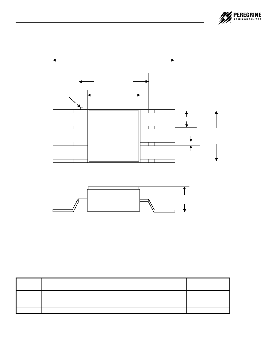
Figure 9. Package Drawing
8 Lead Gullwing Glass Flatpack
Table 4. Ordering Information
Order
Code
Part Marking
Description
Package
Shipping
Method
9304-01 PE9304
PE9304-08CFPG-1A Engineering
Samples
Gullwing Glass Flatpack
20 / Tray
9304-11
PE9304
PE9304-08CFPG-1A Flight Units
Gullwing Glass Flatpack
50 / Tray
9304-00
PE9304-EK
PE9304 Evaluation Kit
Evaluation Kit
1 / Box
TOP VIEW
.050 TYP
.015 TYP
.150 TYP
.380 / .410
.210 / .250
.180 SQ MAX
Pin 1
SIDE VIEW
.070 MAX