
PEREGRINE SEMICONDUCTOR CORP.
|
http://www.peregrine-semi.com
Copyright
Peregrine Semiconductor Corp. 2003
Page 1 of 15
Product Description
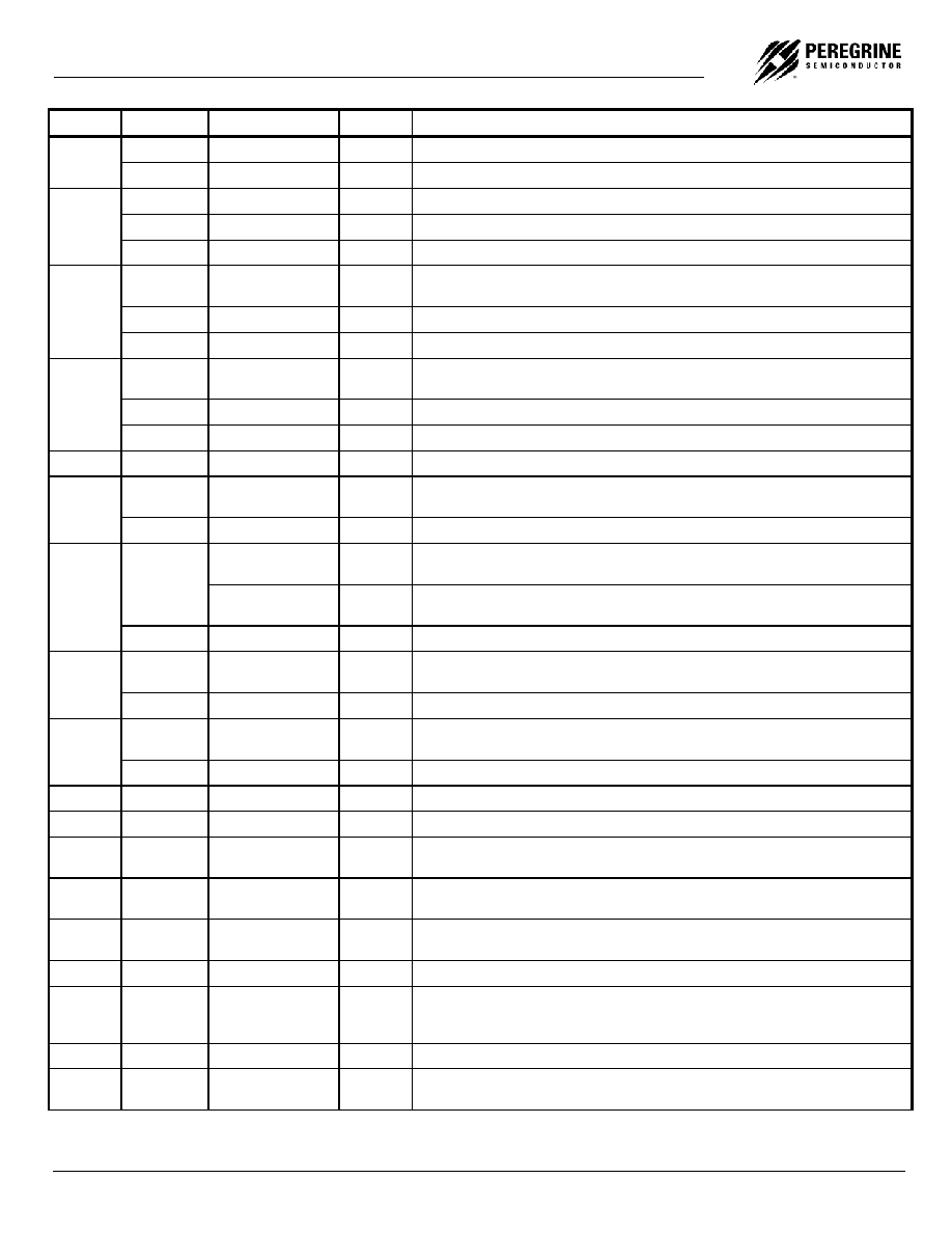
Figure 1. Block Diagram
ADVANCE INFORMATION
PE9702
3.0 GHz Integer-N PLL for Rad
Hard Applications
Features
� 3.0 GHz operation
� �10/11 dual modulus prescaler
� Internal phase detector
� Serial, parallel or hardwired
programmable
� Ultra-low phase noise
� SEU < 10
-9
errors / bit-day
� 100 Krad (Si) total dose
� 44-lead CQFJ
Peregrine's PE9702 is a high-performance integer-N PLL
capable of frequency synthesis up to 3.0 GHz. The
device is designed for superior phase noise performance
while providing an order of magnitude reduction in
current consumption, when compared with existing
commercial space PLLs.
The PE9702 features a 10/11 dual modulus prescaler,
counters and a phase comparator as shown in Figure 1.
Counter values are programmable through either a serial
or parallel interface and can also be directly hard wired.
The PE9702 is optimized for commercial space
applications. Single Event Latch up (SEL) is physically
impossible and Single Event Upset (SEU) is better than
10
-9
errors per bit / day. Fabricated in Peregrine's
patented UTSi� (Ultra Thin Silicon) CMOS technology,
the PE9702 offers excellent RF performance and intrinsic
radiation tolerance.
F
in
F
in
Prescaler
10 / 11
20
Main
Counter
20
Secon-
dary
20-bit
Latch
20
Primary
20-bit
Latch
Pre_en
M(6:0)
A(3:0)
R(3:0)
16
20
R Counter
f
r
Phase
Detector
6
6
f
c
f
p
8
D(7:0)
13
Sdata
PD_U
PD_D

PE9702
Advance Information
Copyright
Peregrine Semiconductor Corp. 2003
File No. 70/0036~00C
|
UTSi CMOS RFIC SOLUTIONS
Page 2 of 15
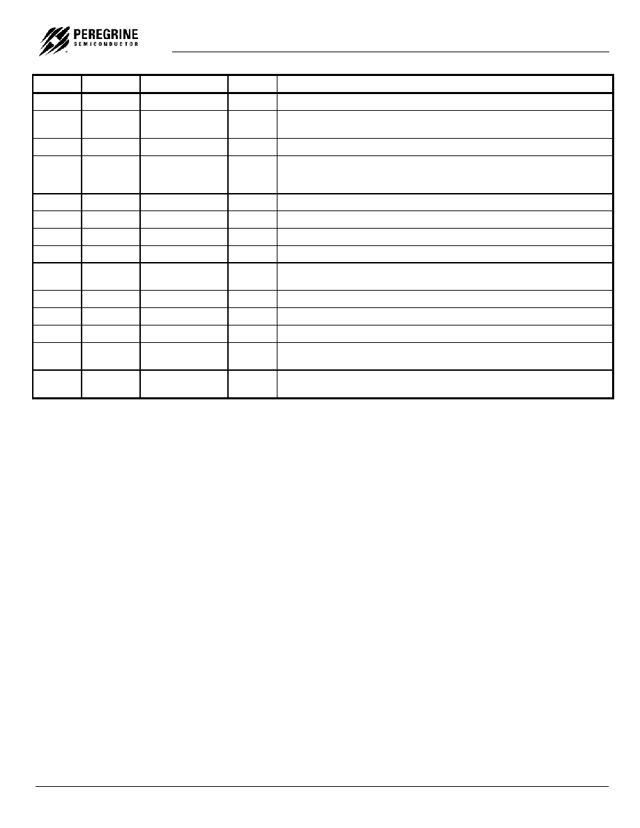
Figure 2. Pin Configuration
Table 1. Pin Descriptions
Pin No.
Pin Name
Interface Mode
Type
Description
1 V
DD
ALL
(Note 1)
Power supply input. Input may range from 2.85 V to 3.15 V. Bypassing recommended.
2 R
0
Direct
Input
R Counter bit0 (LSB).
3 R
1
Direct
Input
R Counter bit1.
4 R
2
Direct
Input
R Counter bit2.
5 R
3
Direct
Input
R Counter bit3.
6 GND ALL
(Note
1)
Ground.
D
0
Parallel
Input
Parallel data bus bit0 (LSB).
7
M
0
Direct
Input
M Counter bit0 (LSB).
8 D
1
Parallel
Input
Parallel data bus bit1.
M
1
Direct
Input
M
Counter
bit1.
9 D
2
Parallel
Input
Parallel data bus bit2.
M
2
Direct
Input
M
Counter
bit2.
10 D
3
Parallel
Input
Parallel data bus bit3.
M
3
Direct
Input
M
Counter
bit3.
11 V
DD
ALL
(Note 1)
Same as pin 1.
12 V
DD
ALL
(Note 1)
Same as pin 1.
13
S_WR Serial
Input
Serial load enable input. While S_WR is "low", Sdata can be serially clocked. Primary
register data is transferred to the secondary register on S_WR or Hop_WR rising edge.
11
12
13
14
15
16
17
10
9
8
7
6
5
4
3
2
1 44 43 42 41 40
35
34
33
32
31
30
29
36
37
38
39
18 19 20 21 22 23 24 25 26 27 28
D
0
, M
0
D
1
, M
1
D
2
, M
2
D
3
, M
3
V
DD
V
DD
S_WR, D
4
, M
4
Sdata, D
5
, M
5
Sclk, D
6
, M
6
FSELS, D
7
, Pre_en
GND
GND
f
p
V
DD
_f
p
D
out
V
DD
C
ext
V
DD
PD_D
PD_U
V
DD
_f
c
f
c
F
in
F
in
Hop
_
WR
A_WR
M1
_W
R
V
DD
Bmo
d
e
S
m
ode, A
3
M2
_W
R
,
A
2
E_WR,
A
1
F
S
EL
P,
A
0
GND
R
3
R
2
R
1
R
0
V
DD
En
h
LD
fr
GND
GND
PE9702
Advance Information
PEREGRINE SEMICONDUCTOR CORP.
|
http://www.peregrine-semi.com
Copyright
Peregrine Semiconductor Corp. 2003
Page 3 of 15
Pin No.
Pin Name
Interface Mode
Type
Description
D
4
Parallel
Input
Parallel data bus bit4
M
4
Direct
Input
M
Counter
bit4
Sdata
Serial
Input
Binary serial data input. Input data entered MSB first.
D
5
Parallel
Input
Parallel data bus bit5.
14
M
5
Direct
Input
M
Counter
bit5.
Sclk Serial
Input
Serial clock input. Sdata is clocked serially into the 20-bit primary register (E_WR
"low") or the 8-bit enhancement register (E_WR "high") on the rising edge of Sclk.
D
6
Parallel
Input
Parallel data bus bit6.
15
M
6
Direct
Input
M
Counter
bit6.
FSELS Serial
Input
Selects contents of primary register (FSELS=1) or secondary register (FSELS=0) for
programming of internal counters while in Serial Interface Mode.
D
7
Parallel
Input
Parallel data bus bit7 (MSB).
16
Pre_en
Direct
Input
Prescaler enable, active "low". When "high", F
in
bypasses the prescaler.
17 GND ALL
Ground.
FSELP Parallel
Input
Selects contents of primary register (FSELP=1) or secondary register (FSELP=0) for
programming of internal counters while in Parallel Interface Mode.
18
A
0
Direct
Input
A Counter bit0 (LSB).
Serial Input
Enhancement register write enable. While E_WR is "high", Sdata can be serially
clocked into the enhancement register on the rising edge of Sclk.
E_WR
Parallel Input
Enhancement register write. D[7:0] are latched into the enhancement register on the
rising edge of E_WR.
19
A
1
Direct
Input
A Counter bit1.
M2_WR Parallel
Input
M2 write. D[3:0] are latched into the primary register (R[5:4], M[8:7]) on the rising edge
of M2_WR.
20
A
2
Direct
Input
A Counter bit2.
Smode Serial,
Parallel Input
Selects serial bus interface mode (
Bmode
=0, Smode=1) or Parallel Interface Mode
(
Bmode
=0, Smode=0).
21
A
3
Direct
Input
A Counter bit3 (MSB).
22
Bmode
ALL
Input
Selects direct interface mode (
Bmode
=1).
23 V
DD
ALL
(Note 1)
Same as pin 1.
24 M1_WR
Parallel
Input
M1 write. D[7:0] are latched into the primary register (
Pre_en
, M[6:0]) on the rising
edge of M1_WR.
25 A_WR
Parallel
Input
A write. D[7:0] are latched into the primary register (R[3:0], A[3:0]) on the rising edge of
A_WR.
26 Hop_WR
Serial,
Parallel
Input
Hop write. The contents of the primary register are latched into the secondary register
on the rising edge of Hop_WR.
27 F
in
ALL
Input
Prescaler input from the VCO. 3.0 GHz max frequency.
28
F
in
ALL Input
Prescaler complementary input. A bypass capacitor in series with a 51
resistor
should be placed as close as possible to this pin and be connected directly to the
ground plane.
29 GND ALL
Ground.
30 f
p
ALL
Output
Monitor pin for main divider output. Switching activity can be disabled through
enhancement register programming or by floating or grounding V
DD
pin 31.
PE9702
Advance Information
Copyright
Peregrine Semiconductor Corp. 2003
File No. 70/0036~00C
|
UTSi CMOS RFIC SOLUTIONS
Page 4 of 15
Pin No.
Pin Name
Interface Mode
Type
Description
31 V
DD
-f
p
ALL
(Note
1)
V
DD
for f
p
. Can be left floating or connected to GND to disable the f
p
output.
32 Dout Serial,
Parallel
Output
Data Out. The MSEL signal and the raw prescaler output are available on Dout through
enhancement register programming.
33 V
DD
ALL
(Note 1)
Same as pin 1.
34 Cext ALL
Output
Logical "NAND" of PD_
U
and PD_
D
terminated through an on chip, 2 k
series
resistor. Connecting Cext to an external capacitor will low pass filter the input to the
inverting amplifier used for driving LD.
35 V
DD
ALL
(Note 1)
Same as pin 1.
36 PD_
D
ALL
Output
PD_
D
is pulse down when f
p
leads f
c
.
37 PD_
U
ALL
PD_
U
is pulse down when f
c
leads f
p
.
38 V
DD
-f
c
ALL
(Note
1)
V
DD
for f
c
. Can be left floating or connected to GND to disable the f
c
output.
39 f
c
ALL
Output
Monitor pin for reference divider output. Switching activity can be disabled through
enhancement register programming or by floating or grounding V
DD
pin 38.
40 GND ALL
Ground.
41 GND ALL
Ground.
42 f
r
ALL
Input
Reference frequency input.
43 LD ALL
Output,
OD
Lock detect and open drain logical inversion of CEXT. When the loop is in lock, LD is
high impedance, otherwise LD is a logic low ("0").
44
Enh
Serial, Parallel
Input
Enhancement mode. When asserted low ("0"), enhancement register bits are
functional.
Note 1:
V
DD
pins 1, 11, 12, 23, 31, 33, 35, and 38 are connected by diodes and must be supplied with the same positive voltage level.
V
DD
pins 31 and 38 are used to enable test modes and should be left floating.
Note 2:
All digital input pins have 70 k
pull-down resistors to ground.
PE9702
Advance Information
PEREGRINE SEMICONDUCTOR CORP.
|
http://www.peregrine-semi.com
Copyright
Peregrine Semiconductor Corp. 2003
Page 5 of 15
Table 2. Absolute Maximum Ratings
Symbol Parameter/Conditions Min Max Units
V
DD
Supply
voltage
-0.3
4.0 V
V
I
Voltage on any input
-0.3
V
DD
+ 0.3
V
I
I
DC into any input
-10
+10
mA
I
O
DC into any output
-10
+10
mA
T
stg
Storage
temperature
range
-65 150
�
C
Table 3. Operating Ratings
Symbol Parameter/Conditions Min Max Units
V
DD
Supply
voltage
2.85
3.15 V
T
A
Operating
ambient
temperature range
-40 85
�
C
Table 4. ESD Ratings
Symbol Parameter/Conditions Level
Units
V
ESD
ESD voltage (Human Body
Model) � Note 1
1000 V
Note 1:
Periodically sampled, not 100% tested. Tested per MIL-
STD-883, M3015 C2
Electrostatic Discharge (ESD) Precautions
When handling this UTSi device, observe the same
precautions that you would use with other ESD-
sensitive devices. Although this device contains
circuitry to protect it from damage due to ESD,
precautions should be taken to avoid exceeding the
rating specified in Table 4.
Latch-Up Avoidance
Unlike conventional CMOS devices, UTSi CMOS
devices are immune to latch-up.

PE9702
Advance Information
Copyright
Peregrine Semiconductor Corp. 2003
File No. 70/0036~00C
|
UTSi CMOS RFIC SOLUTIONS
Page 6 of 15
Table 5. DC Characteristics
V
DD
= 3.0 V, -40
� C < T
A
< 85
� C, unless otherwise specified
Symbol Parameter
Conditions
Min
Typ
Max
Units
I
DD
Operational supply current;
Prescaler disabled
Prescaler enabled
V
DD
= 2.85 to 3.15 V
10
24
31
mA
mA
Digital Inputs: All except f
r
, F
in
,
F
in
V
IH
High level input voltage
V
DD
= 2.85 to 3.15 V
0.7 x V
DD
V
V
IL
Low level input voltage
V
DD
= 2.85 to 3.15 V
0.3 x V
DD
V
I
IH
High level input current
V
IH
= V
DD
= 3.15 V
+70
�
A
I
IL
Low level input current
V
IL
= 0, V
DD
= 3.15 V
-1
�
A
Reference Divider input: f
r
I
IHR
High level input current
V
IH
= V
DD
= 3.15 V
+100
�
A
I
ILR
Low level input current
V
IL
= 0, V
DD
= 3.15 V
-100
�
A
R0 Input: R
0
I
IHR
High level input current
V
IH
= V
DD
= 3.15 V
+70
�
A
I
ILR
Low level input current
V
IL
= 0, V
DD
= 3.15 V
-5
�
A
Counter and phase detector outputs: f
c
, f
p
.
V
OLD
Output voltage LOW
I
out
= 6 mA
0.4
V
V
OHD
Output
voltage
HIGH
I
out
= -3 mA
V
DD
- 0.4
V
Lock detect outputs: Cext, LD
V
OLC
Output voltage LOW, Cext
I
out
= 100 mA
0.4
V
V
OHC
Output voltage HIGH, Cext
I
out
= -100 mA
V
DD
- 0.4
V
V
OLLD
Output voltage LOW, LD
I
out
= 6 mA
0.4
V
PE9702
Advance Information
PEREGRINE SEMICONDUCTOR CORP.
|
http://www.peregrine-semi.com
Copyright
Peregrine Semiconductor Corp. 2003
Page 7 of 15
Table 6. AC Characteristics
V
DD
= 3.0 V, -40
� C < T
A
< 85
� C, unless otherwise specified
Symbol Parameter
Conditions
Min
Max
Units
Control Interface and Latches (see Figures 3, 4, 5)
f
Clk
Serial data clock frequency
(Note 1)
10
MHz
t
ClkH
Serial clock HIGH time
30
ns
t
ClkL
Serial clock LOW time
30
ns
t
DSU
Sdata set-up time after Sclk rising edge, D[7:0] set-up time
to M1_WR, M2_WR, A_WR, E_WR rising edge
10
ns
t
DHLD
Sdata hold time after Sclk rising edge, D[7:0] hold time to
M1_WR, M2_WR, A_WR, E_WR rising edge
10
ns
t
PW
S_WR, M1_WR, M2_WR, A_WR, E_WR pulse width
30
ns
t
CWR
Sclk rising edge to S_WR rising edge. S_WR, M1_WR,
M2_WR, A_WR falling edge to Hop_WR rising edge
30
ns
t
CE
Sclk falling edge to E_WR transition
30
ns
t
WRC
S_WR falling edge to Sclk rising edge. Hop_WR falling
edge to S_WR, M1_WR, M2_WR, A_WR rising edge
30
ns
t
EC
E_WR transition to Sclk rising edge
30
ns
t
MDO
MSEL data out delay after Fin rising edge
C
L
= 12 pf
8
ns
Main Divider (Including Prescaler)
F
in
Operating
frequency
500 3000 MHz
P
Fin
Input level range
External AC coupling
-5
5
dBm
Main Divider (Prescaler Bypassed)
F
in
Operating
frequency
50 300 MHz
P
Fin
Input level range
External AC coupling
-5
5
dBm
Reference Divider
f
r
Operating frequency
(Note 3)
100
MHz
P
fr
Reference input power (Note 2)
Single-ended input
-2
dBm
Phase Detector
f
c
Comparison frequency
(Note 3)
20
MHz
Note 1:
Fclk is verified during the functional pattern test. Serial programming sections of the functional pattern are clocked at 10 MHz to verify Fclk
specification.
Note 2:
CMOS logic levels can be used to drive reference input if DC coupled. Voltage input needs to be a minimum of 0.5V
p-p
.
Note 3:
Parameter is guaranteed through characterization only and is not tested.

PE9702
Advance Information
Copyright
Peregrine Semiconductor Corp. 2003
File No. 70/0036~00C
|
UTSi CMOS RFIC SOLUTIONS
Page 8 of 15
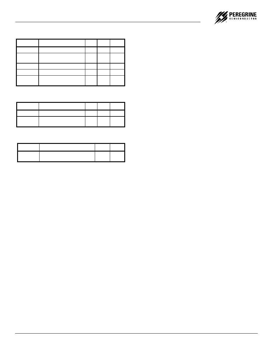
Functional Description
The PE9702 consists of a prescaler, counters, a
phase detector, and control logic. The dual
modulus prescaler divides the VCO frequency by
either 10 or 11, depending on the value of the
modulus select. Counters "R" and "M" divide the
reference and prescaler output, respectively, by
integer values stored in a 20-bit register. An
additional counter ("A") is used in the modulus
select logic. The phase-frequency detector
generates up and down frequency control signals.
The control logic includes a selectable chip
interface. Data can be written via serial bus,
parallel bus, or hardwired directly to the pins. There
are also various operational and test modes and a
lock detect output.
Figure 3. Functional Block Diagram
Control
Logic
R Counter
(6-bit)
Phase
Detector
f
c
PD_U
PD_D
LD
R(5:0)
M(8:0)
A(3:0)
D(7:0)
Sdata
Control
Pins
f
r
Modulus
Select
10/11
Prescaler
M Counter
(9-bit)
Cext
f
p
F
in
F
in

PE9702
Advance Information
PEREGRINE SEMICONDUCTOR CORP.
|
http://www.peregrine-semi.com
Copyright
Peregrine Semiconductor Corp. 2003
Page 9 of 15
Main Counter Chain
Normal Operating Mode
The main counter chain divides the RF input
frequency, F
in
, by an integer derived from the user-
defined values in the "M" and "A" counters. It is
composed of the 10/11 dual modulus prescaler,
modulus select logic, and 9-bit M counter. Setting
Pre_en "low" enables the 10/11 prescaler. Setting
Pre_en "high" allows F
in
to bypass the prescaler
and powers down the prescaler.
The output from the main counter chain, f
p
, is
related to the VCO frequency, F
in
, by the following
equation:
f
p
= F
in
/ [10 x (M + 1) + A] (1)
where A
M + 1, 1 M 511
When the loop is locked, F
in
is related to the
reference frequency, f
r
, by the following equation:
F
in
= [10 x (M + 1) + A] x (f
r
/ (R+1)) (2)
where A
M + 1, 1 M 511
A consequence of the upper limit on A is that F
in
must be greater than or equal to 90 x (f
r
/ (R+1)) to
obtain contiguous channels. Programming the M
Counter with the minimum value of "1" will result in
a minimum M Counter divide ratio of "2".
In Direct Interface Mode, main counter inputs M
7
and M
8
are internally forced low. In this mode, the
M value is limited to 1 M
127.
Prescaler Bypass Mode
Setting Pre_en "high" allows F
in
to bypass and
power down the prescaler. In this mode, the 10/11
prescaler and A register are not active, and the
input VCO frequency is divided by the M counter
directly. The following equation relates F
in
to the
reference frequency, f
r
:
F
in
= (M + 1) x (f
r
/ (R+1)) ) (3)
where 1 M 511
In Direct Interface Mode, main counter inputs M
7
and M
8
are internally forced low. In this mode, the
M value is limited to 1 M
127.
Reference Counter
The reference counter chain divides the reference
frequency, f
r
, down to the phase detector
comparison frequency, f
c
.
The output frequency of the 6-bit R Counter is
related to the reference frequency by the following
equation:
f
c
= f
r
/ (R + 1) (4)
where 0 R 63
Note that programming R with "0" will pass the
reference frequency, f
r
, directly to the phase
detector.
In Direct Interface Mode, R Counter inputs R
4
and
R
5
are internally forced low ("0"). In this mode, the
R value is limited to 0 R 15.
Register Programming
Parallel Interface Mode
Parallel Interface Mode is selected by setting the
Bmode input "low" and the Smode input "low".
Parallel input data, D[7:0], are latched in a parallel
fashion into one of three 8-bit primary register
sections on the rising edge of M1_WR, M2_WR, or
A_WR per the mapping shown in Table 7 on page
10. The contents of the primary register are
transferred into a secondary register on the rising
edge of Hop_WR according to the timing diagram
shown in Figure 5. Data is transferred to the
counters as shown in Table 7 on page 10.
The secondary register acts as a buffer to allow
rapid changes to the VCO frequency. This double
buffering for "ping-pong" counter control is
programmed via the FSELP input. When FSELP is
"high", the primary register contents set the counter
inputs. When FSELP is "low", the secondary
register contents are utilized.
Parallel input data, D[7:0], are latched into the
enhancement register on the rising edge of E_WR
according to the timing diagram shown in Figure 4.
This data provides control bits as shown in Table 8
on page 10 with bit functionality enabled by
asserting the Enh input "low".

PE9702
Advance Information
Copyright
Peregrine Semiconductor Corp. 2003
File No. 70/0036~00C
|
UTSi CMOS RFIC SOLUTIONS
Page 10 of 15
Serial Interface Mode
Serial Interface Mode is selected by setting the
Bmode input "low" and the Smode input "high".
While the E_WR input is "low" and the S_WR input
is "low", serial input data (Sdata input), B
0
to B
19
, is
clocked serially into the primary register on the
rising edge of Sclk, MSB (B
0
) first. The contents
from the primary register are transferred into the
secondary register on the rising edge of either
S_WR or Hop_WR according to the timing diagram
shown in Figure 6. Data is transferred to the
counters as shown in Table 7 on page 10.
The double buffering provided by the primary and
secondary registers allows for "ping-pong" counter
control using the FSELS input. When FSELS is
"high", the primary register contents set the counter
inputs. When FSELS is "low", the secondary
register contents are utilized.
While the E_WR input is "high" and the S_WR input
is "low", serial input data (Sdata input), B
0
to B
7
, is
clocked serially into the enhancement register on
the rising edge of Sclk, MSB (B
0
) first. The
enhancement register is double buffered to prevent
inadvertent control changes during serial loading,
with buffer capture of the serially-entered data
performed on the falling edge of E_WR according to
the timing diagram shown in Figure 5. After the
falling edge of E_WR, the data provides control bits
as shown in Table 8 with bit functionality enabled by
asserting the Enh input "low".
Direct Interface Mode
Direct Interface Mode is selected by setting the
Bmode input "high".
Counter control bits are set directly at the pins as
shown in Table 7. In Direct Interface Mode, main
counter inputs M
7
and M
8
, and R Counter inputs R
4
and R
5
are internally forced low ("0").
Table 7. Primary Register Programming
Interface
Mode
Enh Bmode
Smode R
5
R
4
M
8
M
7
Pre_en M
6
M
5
M
4
M
3
M
2
M
1
M
0
R
3
R
2
R
1
R
0
A
3
A
2
A
1
A
0
M2_WR rising edge load
M1_WR rising edge load
A_WR rising edge load
Parallel 1
0
0
D
3
D
2
D
1
D
0
D
7
D
6
D
5
D
4
D
3
D
2
D
1
D
0
D
7
D
6
D
5
D
4
D
3
D
2
D
1
D
0
Serial* 1
0
1 B
0
B
1
B
2
B
3
B
4
B
5
B
6
B
7
B
8
B
9
B
10
B
11
B
12
B
13
B
14
B
15
B
16
B
17
B
18
B
19
Direct 1
1
X 0 0 0 0
Pre_en M
6
M
5
M
4
M
3
M
2
M
1
M
0
R
3
R
2
R
1
R
0
A
3
A
2
A
1
A
0
*Serial data clocked serially on Sclk rising edge while E_WR "low" and captured in secondary register on S_WR rising edge.
MSB (first in)
(last in) LSB
Table 8. Enhancement Register Programming
Interface
Mode
Enh Bmode
Smode Reserved Reserved Reserved
Power
down
Counter
load
MSEL
output
Prescaler
output
f
c
, f
p
OE
E_WR rising edge load
Parallel 0
0
0
D
7
D
6
D
5
D
4
D
3
D
2
D
1
D
0
Serial* 0
0
1
B
0
B
1
B
2
B
3
B
4
B
5
B
6
B
7
*Serial data clocked serially on Sclk rising edge while E_WR "high" and captured in the double buffer on E_WR falling edge.
MSB (first in)
(last in) LSB

PE9702
Advance Information
PEREGRINE SEMICONDUCTOR CORP.
|
http://www.peregrine-semi.com
Copyright
Peregrine Semiconductor Corp. 2003
Page 11 of 15
Figure 4. Parallel Interface Mode Timing Diagram
Figure 5. Serial Interface Mode Timing Diagram
t
DHLD
t
DSU
t
ClkH
t
ClkL
t
CWR
t
PW
t
WRC
t
EC
t
CE
E_WR
Sdata
Sclk
S_WR
t
DHLD
t
DSU
t
PW
t
CWR
t
WRC
t
PW
D
M1_WR
M2_WR
A_WR
E_WR
Hop_WR
[ ]
0
:
7
PE9702
Advance Information
Copyright
Peregrine Semiconductor Corp. 2003
File No. 70/0036~00C
|
UTSi CMOS RFIC SOLUTIONS
Page 12 of 15
Enhancement Register
The functions of the enhancement register bits are shown below with all bits active "high".
Table 9. Enhancement Register Bit Functionality
Bit Function
Description
Bit 0
Reserved**
Bit 1
Reserved**
Bit 2
Reserved**
Bit 3
Power down
Power down of all functions except programming interface.
Bit 4
Counter load
Immediate and continuous load of counter programming as directed by the
Bmode
and
Smode inputs.
Bit 5
MSEL output
Drives the internal dual modulus prescaler modulus select (MSEL) onto the Dout output.
Bit 6
Prescaler output
Drives the raw internal prescaler output (fmain) onto the Dout output.
Bit 7
f
p
, f
c
OE
f
p
, f
c
outputs disabled.
** Program to 0
Phase Detector
The phase detector is triggered by rising edges
from the main Counter (f
p
) and the reference
counter (f
c
). It has two outputs, namely PD_U, and
PD_D. If the divided VCO leads the divided
reference in phase or frequency (f
p
leads f
c
), PD_D
pulses "low". If the divided reference leads the
divided VCO in phase or frequency (f
r
leads f
p
),
PD_U pulses "low". The width of either pulse is
directly proportional to phase offset between the
two input signals, f
p
and f
c
. The phase detector gain
is 430 mV / radian.
PD_U and PD_D are designed to drive an active
loop filter which controls the VCO tune voltage.
PD_U pulses result in an increase in VCO
frequency and PD_D results in a decrease in VCO
frequency.
A lock detect output, LD is also provided, via the pin
Cext. Cext is the logical "NAND" of PD_U and
PD_D waveforms, which is driven through a series
2k ohm resistor. Connecting Cext to an external
shunt capacitor provides integration. Cext also
drives the input of an internal inverting comparator
with an open drain output. Thus LD is an "AND"
function of PD_U and PD_D. See Figure 3 for a
schematic of this circuit.
PE9702
Advance Information
PEREGRINE SEMICONDUCTOR CORP.
|
http://www.peregrine-semi.com
Copyright
Peregrine Semiconductor Corp. 2003
Page 13 of 15
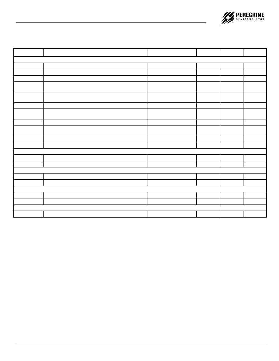
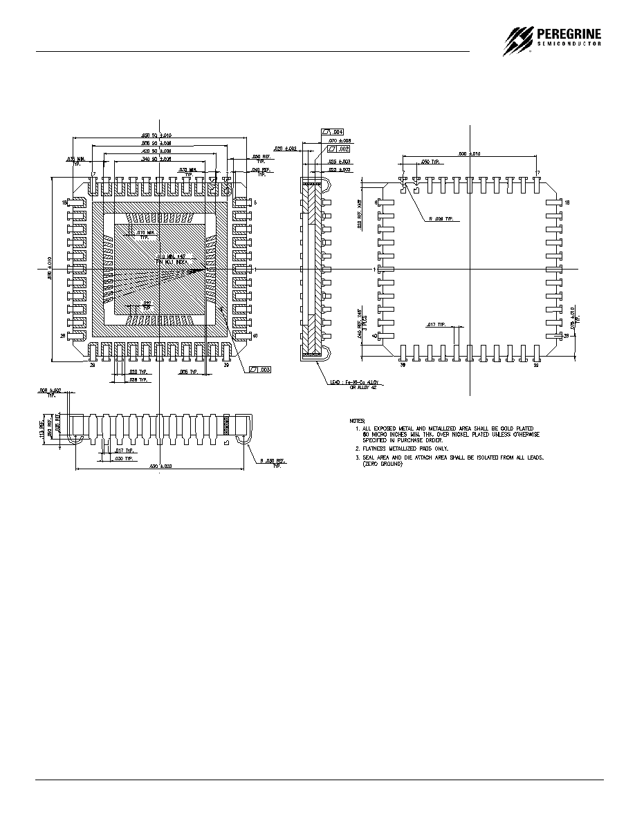
Figure 6. Package Drawing
44-lead CQFJ
All dimensions are in mils
PE9702
Advance Information
Copyright
Peregrine Semiconductor Corp. 2003
File No. 70/0036~00C
|
UTSi CMOS RFIC SOLUTIONS
Page 14 of 15
Table 10. Ordering Information
Order
Code
Part Marking
Description
Package
Shipping
Method
9702-01
PE9702 ES
Engineering Samples
44-pin CQFJ
40 units / Tray
9702-11
PE9702
Flight Units
44-pin CQFJ
40 units / Tray
9702-00
PE9702 EK
Evaluation Kit
1 / Box