 | –≠–ª–µ–∫—Ç—Ä–æ–Ω–Ω—ã–π –∫–æ–º–ø–æ–Ω–µ–Ω—Ç: PE42660 | –°–∫–∞—á–∞—Ç—å:  PDF PDF  ZIP ZIP |

Page 1 of 9
Document No. 70-0192-02
www.psemi.com
©2005 Peregrine Semiconductor Corp. All rights reserved.
The PE42660 is a HaRPTM-enhanced SP6T RF Switch
developed on the UltraCMOSTM process technology. It
addresses the specific design needs of the Quad-Band GSM
Handset Antenna Switch Module Market. On-chip CMOS
decode logic facilitates three-pin low voltage CMOS control,
while high ESD tolerance of 1500 V at all ports, no blocking
capacitor requirements, and on-chip SAW filter over-voltage
protection devices make this the ultimate in integration and
ruggedness.
Peregrine's HaRPTM technology enhancements deliver high
linearity and exceptional harmonics performance. It is an
innovative feature of the UltraCMOSTM process, providing
performance superior to GaAs with the economy and
integration of conventional CMOS.
Preliminary Specification
SP6T UltraCMOSTM 2.75 V Switch
100 ≠ 3000 MHz
Product Description
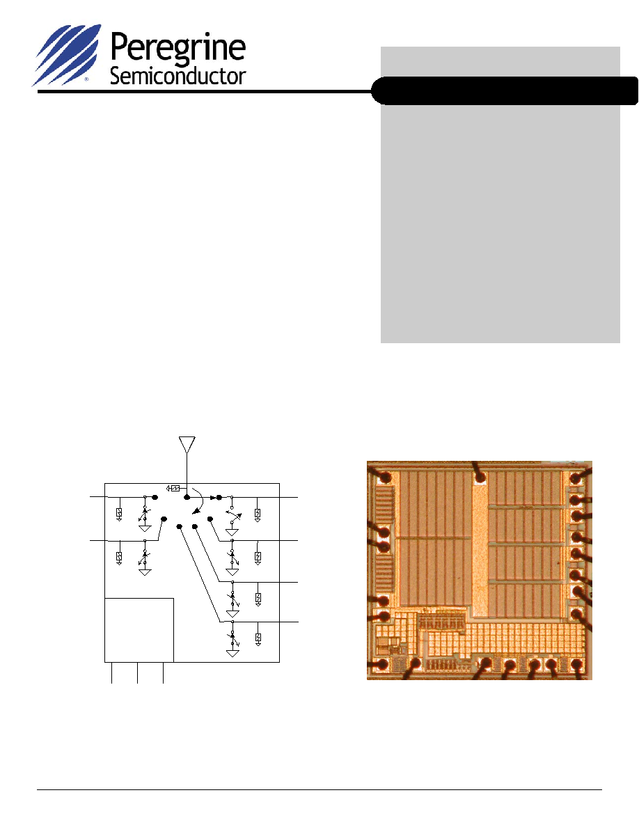
Figure 1. Functional Diagram
Figure 2. Die Top View
PE42660 DIE
Features
ANT
TX1
TX2
GND
GND
RX1
GND
RX2
GND
RX3
GND
RX4
GND
GND
V
DD
V3
GND
V2
V1
GND
GND
RX1
RX2
RX3
RX4
TX1
TX2
CMOS
Control/Driver
and ESD
V1
V2
V3
∑
Three pin CMOS logic control with
integral decoder/driver
∑
Exceptional harmonics performance:
2f
o
= -88 dBc and 3f
o
= -85 dBc
∑
Low TX insertion loss: 0.55 dB at
900 MHz, 0.65 dB at 1900 MHz
∑
TX ≠ RX Isolation of 48 dB at 900 MHz,
40 dB at 1900 MHz
∑
1500 V HBM ESD tolerance all ports
∑
41 dBm P1dB
∑
No blocking capacitors required

Preliminary Specification
PE42660
Page 2 of 9
©2005 Peregrine Semiconductor Corp. All rights reserved.
Document No. 70-0192-02
UltraCMOSTM RFIC Solutions
Table 1. Electrical Specifications @ +25 ∞C, V
DD
= 2.75 V (Z
S
= Z
L
= 50
)
Parameter
Conditions
Typical
Units
Operational Frequency
100-3000
MHz
Insertion Loss
ANT - TX - 850 / 900 MHz
ANT - TX - 1800 / 1900 MHz
ANT - RX - 850 / 900 MHz
ANT - RX - 1800 / 1900 MHz
0.55
0.65
0.90
1.00
dB
dB
dB
dB
Isolation
TX - RX - 850 / 900 MHz
TX - RX - 1800 / 1900 MHz
TX - TX - 850 / 900 MHz
TX - TX - 1800 / 1900 MHz
ANT - TX - 850 / 900 MHz
ANT - TX - 1800 / 1900 MHz
48
40
29
25
31
25
dB
dB
dB
dB
dB
dB
Return Loss
850 / 900 MHz
1800 / 1900 MHz
22
23
dB
2nd Harmonic
35 dBm TX Input - 850 / 900 MHz
33 dBm TX Input - 1800 / 1900 MHz
-88
-85
dBc
3rd Harmonic
35 dBm TX Input - 850 / 900 MHz
33 dBm TX Input - 1800 / 1900 MHz
-85
-84
dBc
Switching Time
(10-90%) (90-10%) RF
2
µ
s
Table 2. Operating Ranges
Note: 1. Assumes RF input period of 4620
µ
s and duty cycle of 50%.
Parameter
Symbol Min Typ Max Units
Temperature range
T
OP
-40
+85
∞C
V
DD
Supply Voltage
V
DD
2.65 2.75 2.85
V
I
DD
Power Supply Current
(V
DD
= 2.75 V)
I
DD
13 20 µA
TX input power
1
(VSWR
3:1)
P
IN
+35
dBm
RX input power
1
(VSWR
1:1)
P
IN
+20
dBm
Control Voltage High
V
IH
0.7 x
V
DD
V
Control Voltage Low
V
IL
0.3 x
V
DD
V

Preliminary Specification
PE42660
Page 3 of 9
Document No. 70-0192-02
www.psemi.com
©2005 Peregrine Semiconductor Corp. All rights reserved.
TX1
PE42660
Die
AN
T
TX2
RX1
RX2
V
DD
V3
V2
V1
GN
D
GND
GND
GND
GND
RX3
GND
GN
D
GN
D
GND
RX4
GND
1
2
3
4
5
6
7
8
9
10 11
12
13
14
15
16
17
18
19
20
Table 3. Pin Descriptions
Notes: 2. Bond wires
should be physically short and connected to
ground plane for best performance.
3. Blocking capacitors needed only when non-zero DC
voltage present.
Figure 3. Pin Configuration (Top View)
Electrostatic Discharge (ESD) Precautions
When handling this UltraCMOSTM device, observe
the same precautions that you would use with
other ESD-sensitive devices. Although this device
contains circuitry to protect it from damage due to
ESD, precautions should be taken to avoid
exceeding the specified rating.
Latch-Up Avoidance
Unlike conventional CMOS devices, UltraCMOSTM
devices are immune to latch-up.
Table 5. Truth Table
Path
V3
V2
V1
ANT ≠ RX1
0
0
0
ANT ≠ RX2
0
0
1
ANT ≠ RX3
0
1
0
ANT ≠ RX4
0
1
1
ANT - TX1
1
0
x
ANT - TX2
1
1
x
Pin No.
Pin Name
Description
1
3
ANT
RF Common ≠ Antenna
2
3
TX1
RF I/O - TX1
3
2
GND
Ground (Requires two bond wires)
4
3
TX2
RF I/O ≠ TX2
5
2
GND
Ground
6
2
GND
Ground
7 V
DD
Supply
8
V3
Switch control input, CMOS logic level
9
2
GND
Ground
10
V2
Switch control input, CMOS logic level
11
V1
Switch control input, CMOS logic level
12
2
GND
Ground
13
2
GND
Ground
14
3
RX4
RF I/O ≠ RX4
15
2
GND
Ground
16
3
RX3
RF I/O ≠ RX3
17
2
GND
Ground
18
3
RX2
RF I/O ≠ RX2
19
2
GND
Ground
20
3
RX1
RF I/O ≠ RX1
Table 4. Absolute Maximum Ratings
Notes: 4. Assumes RF input period of 4620
µ
s and duty cycle of 50%.
5. V
DD
within operating range specified in Table 2.
Part performance is not guaranteed under these
conditions. Exposure to absolute maximum
conditions for extended periods of time may
adversely affect reliability. Stresses in excess of
absolute maximum ratings may cause permanent
damage.
Symbol
Parameter/Conditions
Min
Max Units
V
DD
Power supply voltage
-0.3
4.0
V
V
I
Voltage on any input
-0.3 V
DD
+ 0.3
V
T
ST
Storage temperature range
-65
+150
∞C
P
IN
(50
)
TX input power (50
)
4,5
+38
dBm
RX input power (50
)
4,5
+23
P
IN
(
:1) TX input power (VSWR
:1)
4,5
+35
dBm
V
ESD
ESD Voltage (HBM, MIL_STD
883 Method 3015.7)
1500
V
ESD Voltage at ANT Port
(IEC 61000-4-2)
1700
V

Preliminary Specification
PE42660
Page 4 of 9
©2005 Peregrine Semiconductor Corp. All rights reserved.
Document No. 70-0192-02
UltraCMOSTM RFIC Solutions
Evaluation Kit
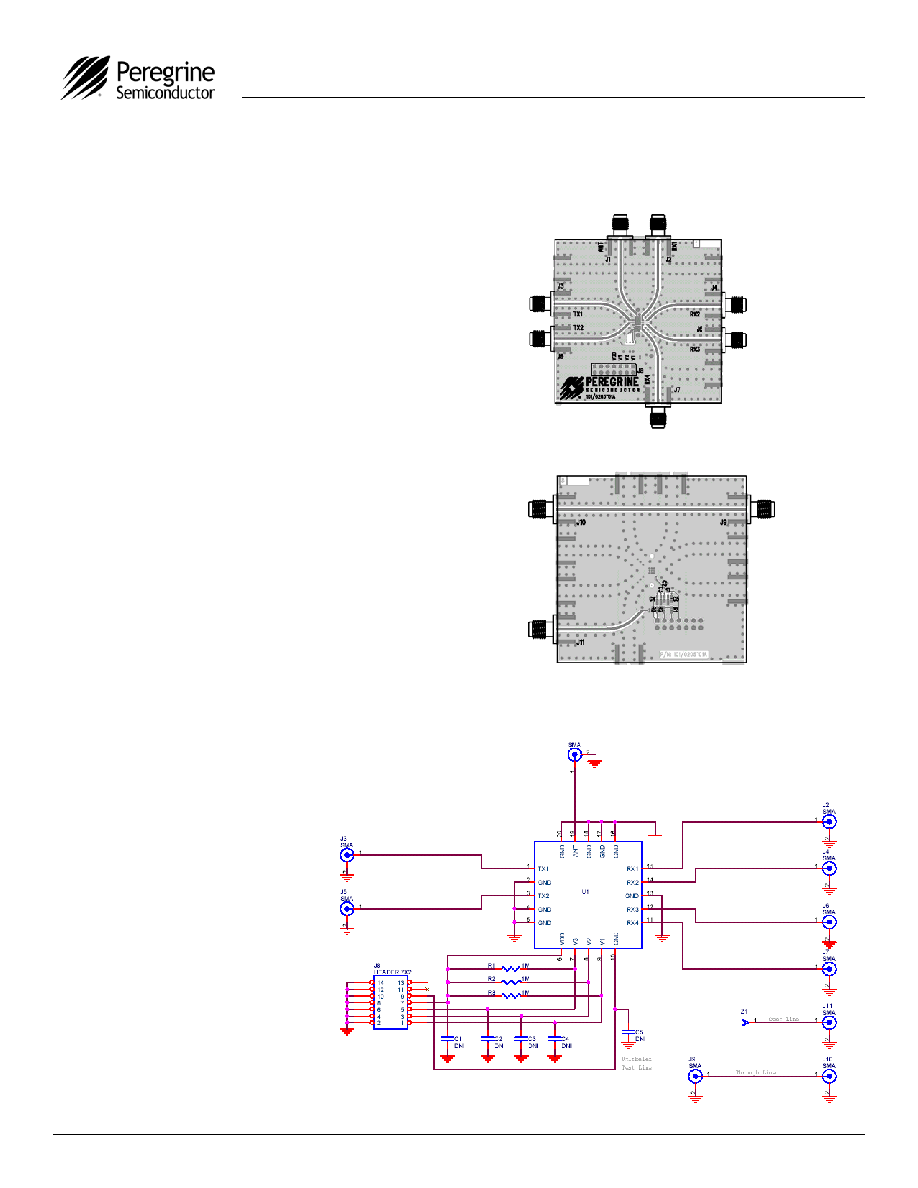
The SP6T Evaluation Kit board was designed to
ease customer evaluation of the PE42660 RF
switch.
The PE42660 has two high power TX ports and four
high isolation RX ports. The TX ports are symmetric
and are designed as paths for the 850, 900, 1800, or
1900 MHz bands. The RX ports are also symmetric
and can be assigned to any of these frequency
bands.
The ANT port connects through a 50
transmission
line to the top SMA connector, J1. The RX and TX
ports connect through 50
transmission lines to
SMA connectors J2 ≠ J7. A through 50
transmission line between SMA connectors J9 and
J10 allows estimation of the PCB losses over
environmental conditions. An open transmission line
connected to J11 is also provided.
J8 supplies DC power to the pin marked V
DD
and the
bottom row of pins, which is GND. 1 M
pull-up
resistors are connected from V
DD
to each of the three
control logic inputs: V1, V2, and V3. These pull-up
resistors are provided for ease of evaluation on this
board and are not required for the PE42660 to
operate.
Adding a jumper between a control pin and the
adjacent GND pin on the bottom row of J8 will set a
logic-0 on that control pin. Removing the jumper will
set a logic-1. To evaluate the PE42660, add or
remove jumpers according to the truth table in
Table 5.
Figure 4. Evaluation Board Layout
ANT RX1
RX2
RX3
RX4
TX1
TX2
Open Line
Through-Line
Figure 5. Evaluation Board Schematic
Peregrine Specification 101/0205
Peregrine Specification 102/0267

Preliminary Specification
PE42660
Page 5 of 9
Document No. 70-0192-02
www.psemi.com
©2005 Peregrine Semiconductor Corp. All rights reserved.
Electrical Test and Performance Specifications
PE42660 dice are 100% electrically tested for the
parameters listed below from
Table 1 and Table 2. All
other parameters are guaranteed through design and
characterization.
Wafer and Die Packaging
Peregrine Semiconductor has two methods for shipping
dice to our customers. The shipping option used is
based on the customer's requirements and the number
of dice.
Peregrine offers product dice in two packaging options:
Standard Die Carrier Packages (waffle pack) and dice
on Film Frames.
Wafer Mount/Dicing
In preparation for dicing, wafers are thinned and
polished and 100% electrically probed prior to
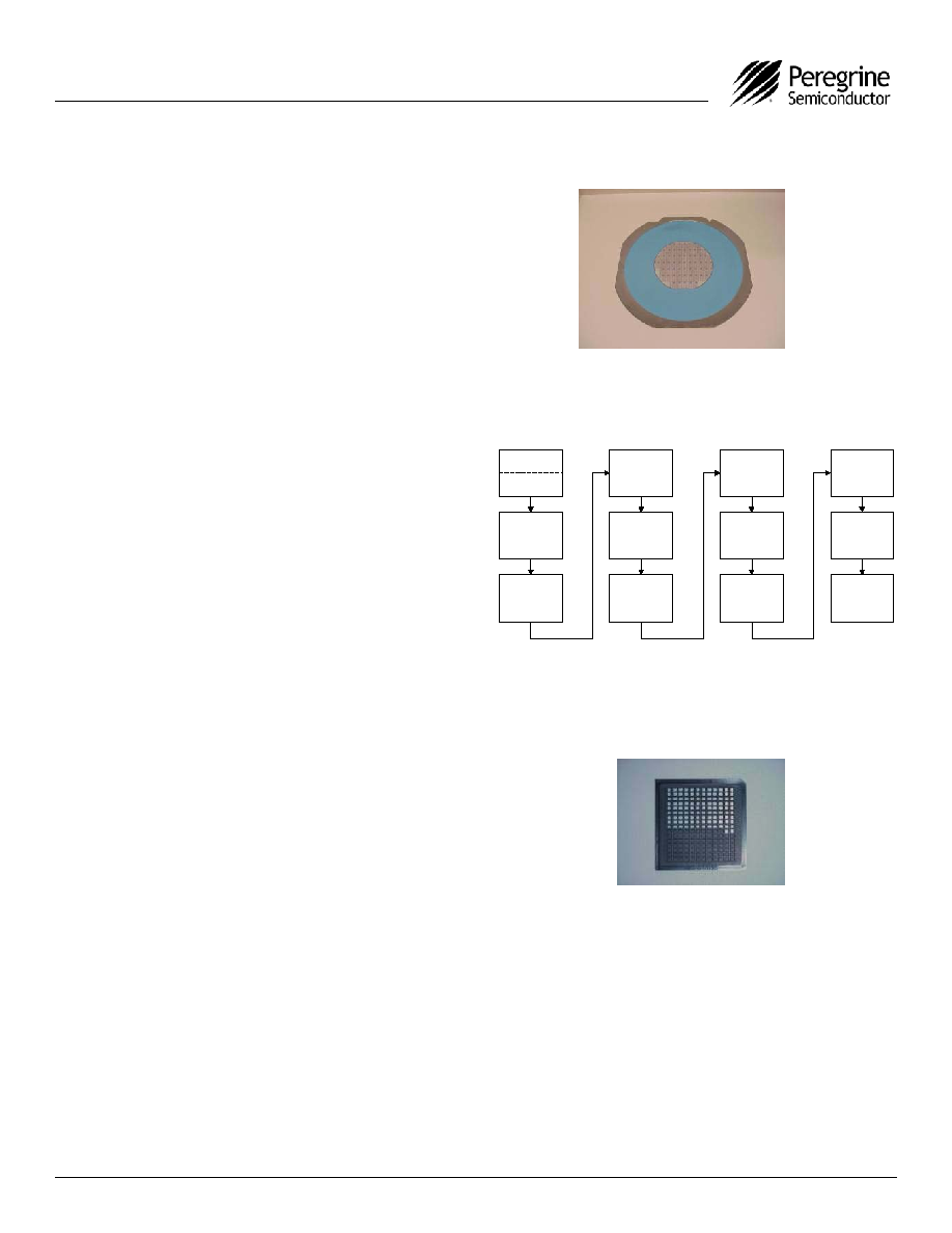
mounting on film frame tape and rings. Figure 6 shows
a wafer mounted on film frame using PVC backed
mounting tape. In preparation for shipment, wafers are
visually inspected after singulation and shipped with an
electronic map file providing good dice locations.
∑
Insertion Loss (all ports)
∑
TX1 & TX2 Harmonics
∑
TX ≠ RX Isolation
∑
I
DD
supply current
∑
Control pin leakages
Storage and Preservation
Proper storage conditions are necessary to prevent
product contamination and/or degradation after
shipment.
Product should be stored in the original unopened
packaging or, once opened, in a nitrogen purged
cabinet at room temperature (45% + 15% relative
humidity controlled environment).
Singulated wafers mounted on film frames are intended
for immediate use and have a limited shelf life. This is
primarily due to the nature of the adhesive tape used
for mounting the product. This product can be stored
up to 30 days. This applies whether or not the material
has remained in its original sealed container. To reduce
the risk of contamination or degradation, it is
recommended that product not being used in the
assembly process be returned to their original
containers and resealed with a vacuum seal process.
Figure 6. Wafer on Film Frame
Figure 8. Waffle Pack
Wafer
Processing
Visual
Inspection
Process Control
Monitor (PCM)
Wafer Level
Reliability (WLR)
Backgrind
and Polish
Dice Picking
100%
Electrical Test
Ink Reject Die or
Electronic Wafer
Map
Outgoing QA
Inspection
Wafer
Singulation
100% Visual
Inspection
Pack and Ship
Wafers
Carrier Loading
Pack and Ship
Dice
Figure 7. Dice and Wafer Processing Flow
Standard Die Carrier Package/Waffle Pack
Waffle packs are available to customers during product
development and prototyping phase only. Orders will
move to film frames at production launch or for large
quantity requirements.
Dice have been 100% electrically probed, singulated,
visually inspected and are packaged in a 2"x2" waffle
pack (400 dice per waffle pack).
