 | –≠–ª–µ–∫—Ç—Ä–æ–Ω–Ω—ã–π –∫–æ–º–ø–æ–Ω–µ–Ω—Ç: PI3A4629 | –°–∫–∞—á–∞—Ç—å:  PDF PDF  ZIP ZIP |
1
PS8717 12/15/03
Features
∑ Low On-Resistance: 0.4 Max (+2.7V Supply)
∑ 0.1 Max. On-Resistance Flatness at +25∞C
∑ Fast Switching: 10ns Max.
∑ +1.5V to +3.6V Single-Supply Operation
∑ TTL/CMOS-Logic Compatible
∑ ≠25dB Off-Isolation at 100KHz
∑ 1nA Max. Off-Leakage at +25∞C
∑ Packaging (Pb-free available):
≠ 5-pin Small Compact SOT-23
≠ 6-contact Ultra Compact Thin Dual in-line Flat No Lead
TDFN
Applications
∑ Cellular Phones ∑ Communications Circuits
∑ Battery-Operated Equipment ∑ DSL Modems
∑ Audio and Video Signal Routing ∑ PCMCIA Cards
Description
PI3A4629 is a single-pole/single-throw (SPST) normally open
(NO) analog switch that operates from a single +1.5V to +3.6V
supply.
The switch has 0.4 Max On-Resistance (R
ON
), with 0.1 Max
R
ON
flatness over the analog signal range when powered from a
+3.0V supply. Leakage currents are less than 2nA and fast switch-
ing times are less than 10ns.
To minimize PC board area use, the device is available in the
ultra compact TDFN and the small compact SOT-23 packages.
The PI3A4629 pinout is optimized for the highest package off-
isolation available.
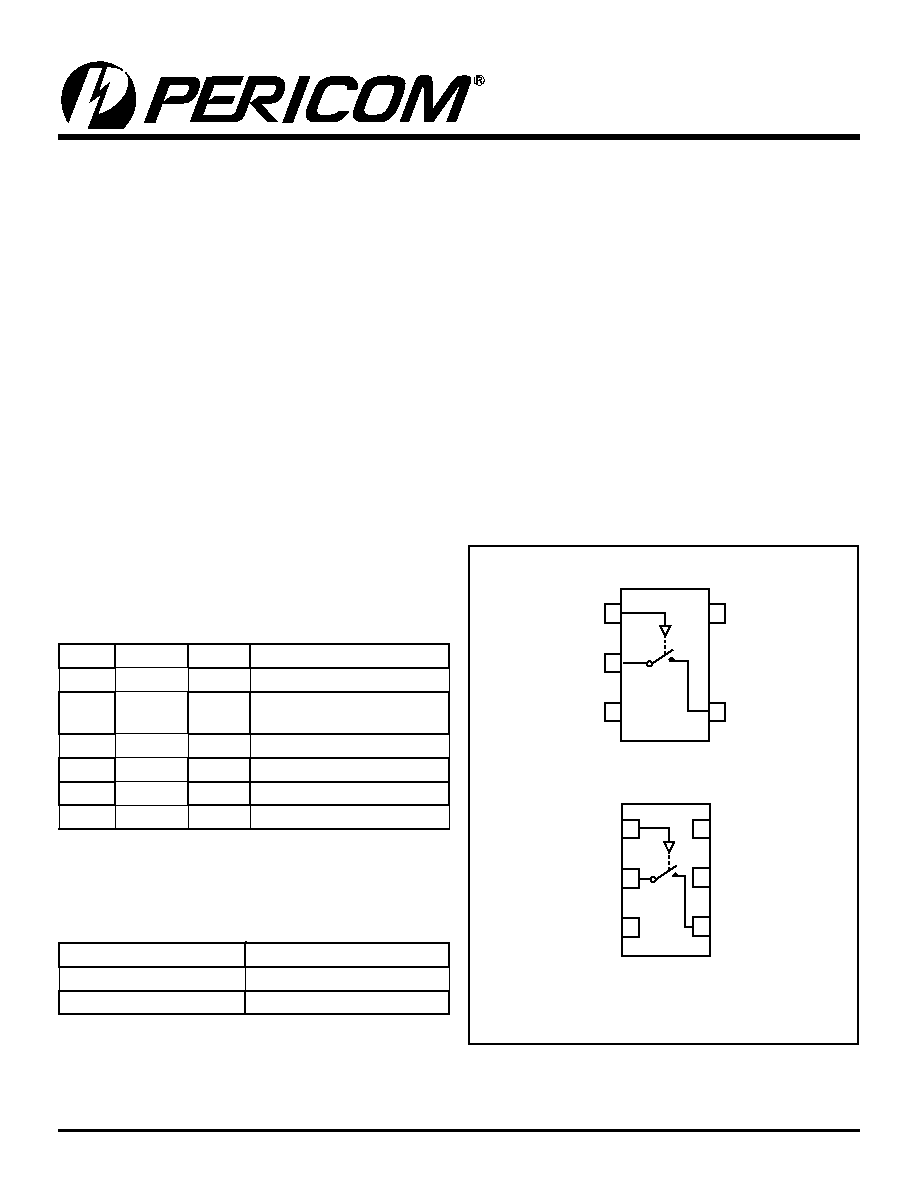
Functional Block Diagrams/Pin Configurations
Top Views
Switches shown for Logic "0" input
PI3A4629
3.0V, SOT
INYTM
Single-Supply
0.4 SPST (NO) CMOS Analog Switch
Pin Description
Note:
NO and COM pins are identical and interchangeable. Any pin may be
considered as an input or an output; signals pass.
Truth Table
COM
NO
GND
1
2
3
5
4
V
CC
IN
SOT23
IN
COM
GND
1
2
3
6
4
V
CC
NO
5 N.C.
TDFN
N.C. = No Internal Connection
TDFN
SOT-23
Name
Function
2
2
COM
Analog Switch, Common
4
4
NO
Analog Switch, Normally
Open
3
3
GND
Ground
1
1
IN
Digital Control Input
6
5
V
CC
Positive Supply Voltage
5
-
N.C.
No Internal Connection
Input
Switch State
LOW
OFF
HIGH
ON

PI3A4629
3.0V, SOT
INY
TM Single-Supply
0.4 SPST (NO) CMOS Analog Switch
2
PS8717 12/15/03
Caution: Stresses beyond those listed under "Absolute Maximum Ratings" may cause permanent damage to the device. This is a
stress only rating and operation of the device at these or any other conditions beyond those indicated in the operational sections of
this specification is not implied.
Absolute Maximum Ratings
Voltages Referenced to GND
V
CC
......................................................................≠0.5V to +3.6V
V
IN
, V
COM
, V
NC
, V
NO
(Note 1)..................≠0.5V to V
CC
+0.3V
or 30mA, whichever occurs first
Current (any terminal).....................................................±200mA
Peak Current, COM, NO, NC
(Pulsed at 1ms, 10% duty cycle).....................................±400mA
Note 1: Signals on NC, NO, COM, or IN exceeding V
CC
or GND are clamped by internal diodes. Limit forward diode current to
Thermal Information
Continuous Power Dissipation
SOT-23 (derate 7.1mW/∫C above +70∫C)........................... 0.5W
Storage Temperature ........................................≠65∫C to +150∫C
Lead Temperature (soldering, 10s) ................................. +300∫C
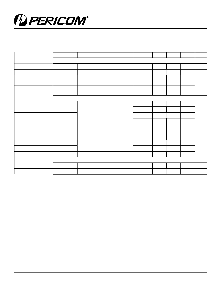
Electrical Specifications - Single +3.3V Supply
(V
CC
= +3.3V ± 10%, GND = 0V, V
IH
= 1.4V, V
IL
= 0.5V)
Description
Parameters
Test Conditions
Temp.(∞C) Min.
(1)
Typ.
(2)
Max.
(1)
Units
Analog Switch
Analog Signal Range
(3)
V
ANALOG
Full
0
V
CC
V
On Resistance
R
ON
V
CC
= 2.7V, I
COM
= 100mA,
V
NO
or V
NC
= 1.5V
25
0.4
Full
0.4
On-Resistance Match
Between Channels
(4)
R
ON
25
0.05
Full
0.06
On-Resistance Flat-
ness
(5)
R
FLAT(ON)
V
CC
=2.7V, I
COM
= 100mA,
V
NO
or V
NC
=0.8V, 2.0V
25
0.1
Full
0.1
NO or NC Off Leakage
Current
(6)
I
COM(OFF)
or
I
NC(OFF)
V
CC
=3.3V, V
COM
= 0V,
V
NO
or V
NC
= +2.0V
25
≠1
1
nA
Full
≠20
10
COM On Leakage Cur-
rent
(6)
I
COM(ON)
V
CC
=3.3V, V
COM
= +2.0V
V
NO
or V
NC
=+ 2.0V
25
≠2
2
Full
≠20
20
PI3A4629
3.0V, SOT
INY
TM Single-Supply
0.4 SPST (NO) CMOS Analog Switch
3
PS8717 12/15/03
Electrical Specifications - Single +3.3V Supply
(continued)
(V
CC
= + 3.3V ± 10%, GND = 0V, V
IH
= 1.4 V, V
IL
= 0.5V)
Notes:
1. The algebraic convention, where most negative value is a minimum and most positive is a maximum, is used in this data sheet.
2. Typical values are for DESIGN AID ONLY, not guaranteed or subject to production testing.
3. Guaranteed by design.
4. R
ON
=
R
ON
Max. - R
ON
Min.
5. Flatness is defined as the difference between the maximum and minimum value of On-Resistance measured.
6. Leakage parameters are 100% tested at maximum rated hot temperature and guaranteed by correlation at +25∫C.
7. Off Isolation = 20log
10
[ V
COM
/ (V
NO
or V
NC
)
]. See Figure 3.
Description
Parameters
Test Conditions
Temp (∫C) Min.
(1)
Typ.
(2)
Max.
(1)
Units
Logic Input
Input High Voltage
V
IH
Guaranteed logic High Level
Full
1.4
V
Input Low Voltage
V
IL
Guaranteed logic Low Level
0.5
Input Current with Volt-
age High
I
INH
V
IN
= 1.4V, all others = 0.5V
≠1
1
µA
Input Current with Volt-
age Low
I
INL
V
IN
= 0.5V, all other = 1.4V
≠1
1
Dynamic
Turn-On Time
t
ON
V
CC
= 3.3V, V
NO
or
V
NC
= 2.0V, Figure 1
25
10
ns
Full
10
Turn-Off Time
t
OFF
25
10
Full
10
Charge Injection
(3)
Q
C
L
= 1nF, V
GEN
= 0V,
R
GEN
= 0, Figure 2
25
50
pC
Off Isolation
(7)
O
IRR
RL = 50, f = 100 KHz, Figure 3
-25
dB
NC or NO Capacitance
C
(OFF)
f = 1MHz, Figure 4
130
pF
COM Off Capacitance
C
COM(OFF)
130
COM On Capacitance
C
COM(ON)
f = 1MHz, Figure 4
270
Supply
Power-Supply Range
V
CC
Full
1.5
3.6
V
Positve Supply Current
I
CC
V
CC
= 3.6V, V
IN
= 0V or V
CC
100
nA

PI3A4629
3.0V, SOT
INY
TM Single-Supply
0.4 SPST (NO) CMOS Analog Switch
4
PS8717 12/15/03
Electrical Specifications - Single +2.5V Supply
(V
CC
= +2.5V ± 10%, GND = 0V, V
IH
= 1.4V, V
IL
= 0.5V)
Notes:
1. The algebraic convention, where most negative value is a minimum and most positive is a maximum, is used in this data sheet.
2. Typical values are for DESIGN AID ONLY, not guaranteed or subject to production testing.
3. Guaranteed by design.
4. R
ON
=
R
ON
max. - R
ON
min.
5. Flatness is defined as the difference between the maximum and minimum value of On-resistance measured.
Description
Parameters
Test Conditions
Temp.(∞C) Min.
(1)
Typ.
(2)
Max.
(1)
Units
Analog Switch
Analog Signal Range
(3)
V
ANALOG
0
V
CC
V
On Resistance
R
ON
V
CC
= 2.5V, I
COM
= ≠8mA,
V
NO
or V
NC
= 1.8V
25
0.4
Full
0.4
On-Resistance Match
Between Channels
(4)
R
ON
V
CC
= 2.5V, I
COM
= ≠8mA,
V
NO
or V
NC
= 0.8V,1.8V
25
0.05
Full
0.06
On-Resistance Flatness
(5)
R
FLAT(ON)
25
0.1
Full
0.1
Dynamic
Turn-On Time
t
ON
V
CC
= 2.5V, V
NO
or V
NC
=
1.8V, Figure 1
25
10
ns
Full
15
Turn-Off Time
t
OFF
25
10
Full
10
Charge Injection
(3)
Q
C
L
= 1nF, V
GEN
= 0V,
R
GEN
= 0V, Figure 2
25
42
pC
Logic Input
Input HIGH Voltage
V
IH
Guaranteed logic high level
Full
1.4
V
Input LOW Voltage
V
IL
Guaranteed logic Low level
Full
0.5
Input HIGH Current
I
INH
V
IN
= 1.4V, all others = 0.5V
Full
≠1
1
µA
Input HIGH Current
I
INL
V
IN
= 0.5V, all others = 1.4V
Full
≠1
1

PI3A4629
3.0V, SOT
INY
TM Single-Supply
0.4 SPST (NO) CMOS Analog Switch
5
PS8717 12/15/03
Electrical Specifications - Single +1.8V Supply
(V
CC
= +1.8V ± 10%, GND = 0V, V
IH
= 1.4V, V
IL
= 0.5V)
Notes:
1. The algebraic convention, where most negative value is a minimum and most positive is a maximum, is used in this data sheet.
2. Typical values are for DESIGN AID ONLY, not guaranteed or subject to production testing.
3. Guaranteed by design.
4. R
ON
=
R
ON
max. - R
ON
min.
5. Flatness is defined as the difference between the maximum and minimum value of On-resistance measured.
Description
Parameters
Test Conditions
Temp.(∞C) Min.
(1)
Typ.
(2)
Max.
(1)
Units
Analog Switch
Analog Signal
Range
(3)
V
ANALOG
0
V
CC
V
On-Resistance
R
ON
V
CC
= 1.8V, I
COM
= ≠4mA,
V
NO
or V
NC
= 1.5V
25
0.4
Full
0.8
On-Resistance
Match Between
Channels
(4)
R
ON
V
CC
= 1.8V, I
COM
= ≠4mA,
V
NO
or V
NC
= 0.8V,1.5V
25
0.05
Full
0.06
On-Resistance Flat-
ness
(5)
R
FLAT(ON)
25
0.4
Full
0.6
Dynamic
Turn-On Time
t
ON
V
CC
= 1.8V, V
NO
or V
NC
= 1.5V,
Figure 1
25
15
ns
Full
15
Turn-Off Time
t
OFF
25
10
Full
15
Charge Injection
(3)
Q
C
L
= 1nF, V
GEN
= 0V, R
GEN
= 0V,
Figure 2
25
29
pC
Logic Input
Input HIGH Voltage
V
IH
Guaranteed logic high level
Full
1.4
V
Input LOW Voltage
V
IL
Guaranteed logic Low level
Full
0.5
Input HIGH Current
I
INH
V
IN
= 1.4V, all others = 0.5V
Full
≠1
1
µA
Input HIGH Current
I
INL
V
IN
= 0.5V, all others = 1.4V
Full
≠1
1