1
PS8162F 09/23/04
Function
BE
A
0≠7
Disconnect
H
Hi-Z
Connect
L
B
0≠7
Truth Table
(1)
Notes:
H = High Voltage Level
L = Low Voltage Level
Hi-Z = High Impedance
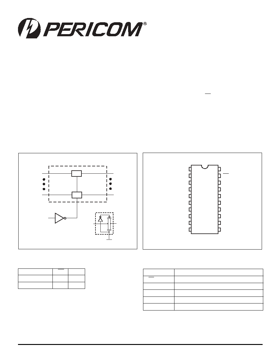
Block Diagram
Pin Description
Pin Name
Description
BE
Bus Enable Input (Active LOW)
A0≠7
Bus A
B0≠7
Bus B
GND
Ground
V
CC
Power
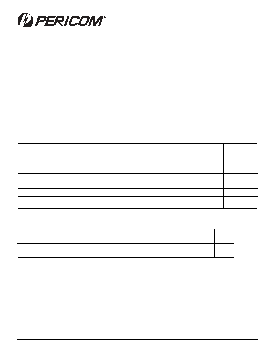
Pin Configuration
PI3B3245
3.3V, Hot Insertion
8-Bit, 2-Port, NanoSwitchTM
12345678901234567890123456789012123456789012345678901234567890121234567890123456789012345678901212345678901234567890123456789012123456789012
12345678901234567890123456789012123456789012345678901234567890121234567890123456789012345678901212345678901234567890123456789012123456789012
Features
∑ Near-Zero propagation delay
∑ 5-ohm switches connect inputs to outputs
∑ Fast Switching Speed - 4.5ns max.
∑ Ultra Low Quiescent Power (0.2µA Typical)
≠ Ideally suited for notebook applications
∑ TTL-compatible control of inputs levels
∑ Packaging (Pb-free & Green available):
≠ 20-pin QSOP (Q)
≠ 20-pin TSSOP (L)
≠ 20-pin SOIC (S)
Description
Pericom Semiconductor's PI3B3245 is a 3.3V 8-bit, 2-port bus switch
designed with a low On-Resistance (5-ohm) allowing inputs to be
connected directly to outputs. The bus switch creates no additional
propagational delay or additional ground bounce noise. The switches
are turned ON by the Bus Enable (BE) input signal.
V
CC
NC
1
20
BE
A
0
2
19
B
0
A
1
3
18
B
1
A
2
4
17
B
2
A
3
5
16
B
3
A
4
6
15
B
4
A
5
7
14
B
5
A
6
8
13
B
6
A
7
9
12
B
7
GND
10
11
A
7
A
0
B
7
B
0
BE
SW
SW
A
A
B
BE
SW
PI3B3245
3.3V, Hot Insertion
8-Bit, 2-Port, NanoSwitchTM
2
PS8162F 09/23/04
12345678901234567890123456789012123456789012345678901234567890121234567890123456789012345678901212345678901234567890123456789012123456789012
12345678901234567890123456789012123456789012345678901234567890121234567890123456789012345678901212345678901234567890123456789012123456789012
12345678901234567890123456789012123456789012345678901234567890121234567890123456789012345678901212345678901234567890123456789012123456789012
12345678901234567890123456789012123456789012345678901234567890121234567890123456789012345678901212345678901234567890123456789012123456789012
Capacitance
(T
A
= 25∞C, f = 1 MHz)
Parameters
(4)
Description
Test Conditions
Typ.
Units
C
IN
Input Capacitance
V
IN
= 0V
3.0
pF
C
OFF
A/B Capacitance, Switch Off
V
IN
= 0V
8.0
pF
C
ON
A/B Capacitance, Switch On
V
IN
= 0V
16.0
pF
DC Electrical Characteristics
(Over the Operating Range, T
A
= ≠40∞C to +85∞C, V
CC
=3.3V ±10%)
Parameters Description
Test Conditions
(1)
Min. Typ
(2)
Max.
Units
V
IH
Input HIGH Voltage
Guaranteed Logic HIGH Level
2.0
V
V
IL
Input LOW Voltage
Guaranteed Logic LOW Level
≠0.5
0.8
V
I
IH
Input HIGH Current
V
CC
= Max., V
IN
= V
CC
±1
µA
I
IL
Input LOW Current
V
CC
= Max., V
IN
= GND
±1
µA
I
OZH
High Impedance Output Current 0
I
N
, Y
N
V
CC
±1
µA
V
IK
Clamp Diode Voltage
V
CC
= Min., I
IN
= ≠18mA
≠1.2
V
R
ON
Switch On Resistance
(3)
V
CC
= Min., V
IN
= 0.0V, I
ON
= 48mA or 64mA
5
8
V
CC
= Min., V
IN
= 2.4V,I
ON
= 15mA
10
17
Notes:
1. For Max. or Min. conditions, use appropriate value specified under Electrical Characteristics for the applicable device type.
2. Typical values are at V
CC
= 3.3V, T
A
= 25∞C ambient and maximum loading.
3. Measured by the voltage drop betweenAand B pin at indicated current through the switch. ON resistance is determined
by the lower of the voltages on the two (A,B) pins.
4. This parameter is determined by device characterization but is not production tested.
Storage Temperature ..................................................................... ≠65∞C to +150∞C
Ambient Temperature with Power Applied ..................................... ≠40∞C to +85∞C
Supply Voltage to Ground Potential ................................................. ≠0.5V to +4.6V
DC Input Voltage .............................................................................. ≠0.5V to +4.6V
DC Output Current ....................................................................................... 120mA
Power Dissipation ............................................................................................ 0.5W
Note:
Stresses greater than those listed under MAXIMUM RATINGS may cause permanent
damage to the device. This is a stress rating only and functional operation of the device
at these or any other conditions above those indicated in the operational sections of this
specification is not implied. Exposure to absolute maximum rating conditions for
extended periods may affect reliability.
Maximum Ratings
(Above which the useful life may be impaired. For user guidelines, not tested.)
PI3B3245
3.3V, Hot Insertion
8-Bit, 2-Port, NanoSwitchTM
3
PS8162F 09/23/04
12345678901234567890123456789012123456789012345678901234567890121234567890123456789012345678901212345678901234567890123456789012123456789012
12345678901234567890123456789012123456789012345678901234567890121234567890123456789012345678901212345678901234567890123456789012123456789012
PI3B3245
Com.
Parameters Description
Conditions
(1)
Min.
Max. Units
t
PLH
Propagation Delay
(2,3)
C
L
= 50pF
t
PHL
Ax to Bx, Bx to Ax
R
L
= 500
0.25
ns
t
PZH
Bus Enable Time
C
L
= 50pF,
t
PZL
BE to Ax or Bx
R
L
= 500
,
1.0
4.0
ns
t
PHZ
Bus Disable Time
R
L
= 500
t
PLZ
BE to Ax or Bx
1.0
4.5
ns
Power Supply Characteristics
Parameters Description
Test Conditions
(1)
Min.
Typ
(2)
Max.
Units
I
CC
Quiescent Power
V
CC
= Max.
V
IN
= GND or V
CC
0.1
3.0
µA
Supply Current
I
CC
Supply Current per
V
CC
= Max.
V
IN
= 3.0V
(3)
750
µA
Input HIGH
Notes:
1. For Max. or Min. conditions, use appropriate value specified under Electrical Characteristics for the applicable device.
2. Typical values are at V
CC
= 3.3V, +25∞C ambient.
3. Per TTL driven input (control input only); A and B pins do not contribute to I
CC
.
Switching Characteristics over Operating Range
Notes:
1. See test circuit and waveforms.
2. This parameter is guaranteed but not tested on Propagation Delays.
3. The bus switch contributes no propagational delay other than the RC delay of the ON
resistance of the switch and the load capacitance. The time constant for the switch alone is
of the order of 0.25ns for 50pF load. Since this time constant is much smaller than the rise/
fall times of typical driving signals, it adds very little propagational delay to the system.
Propagational delay of the bus switch when used in a system is determined by the driving
circuit on the driving side of the switch and its interaction with the load on the driven side.
Applications Information
Logic Inputs
The logic control inputs can be driven up to +3.6 regardless of the supply voltage. For example, given a + 3.3V supply, IN may be
driven low to 0V and high to 3.6V. Driving IN Rail-to-RailÆ minimizes power consumption.
Power-Supply Sequencing and Hot-Plug Information
Proper power-supply sequencing is recommended for all CMOS devices. Always apply V
CC
and GND before applying signals to
input/output or control pins.
Rail-to-Rail is a registeredtrademark of Nippon Motorola, Ltd

PI3B3245
3.3V, Hot Insertion
8-Bit, 2-Port, NanoSwitchTM
4
PS8162F 09/23/04
12345678901234567890123456789012123456789012345678901234567890121234567890123456789012345678901212345678901234567890123456789012123456789012
12345678901234567890123456789012123456789012345678901234567890121234567890123456789012345678901212345678901234567890123456789012123456789012
12345678901234567890123456789012123456789012345678901234567890121234567890123456789012345678901212345678901234567890123456789012123456789012
12345678901234567890123456789012123456789012345678901234567890121234567890123456789012345678901212345678901234567890123456789012123456789012
.337
.344
.053
.069
.004
.010
SEATING
PLANE
.025
BSC
.007
.010
.228
.244
.150
.157
1
20
.016
.050
X.XX
X.XX
DENOTES DIMENSIONS
IN MILLIMETERS
0.635
8.56
8.74
1.35
1.75
5.79
6.19
0.41
1.27
0.101
0.254
.008
.012
0.203
0.305
3.81
3.99
0.178
0.254
.058
1.47
.015 x 45∞
0.38
REF
Detail A
Detail A
.008
0.20
MIN.
Guage Plane
.010
0.254
.041
1.04
REF
.016
.035
0.41
0.89
0∞-6∞
.008
.013
0.20
0.33
.252
.260
.047
1.20
.002
.006
SEATING
PLANE
.0256
BSC
.018
.030
.004
.008
.238
.269
1
20
.169
.177
X.XX
X.XX
DENOTES CONTROLLING
DIMENSIONS IN MILLIMETERS
0.05
0.15
6.1
6.7
0.45
0.75
0.09
0.20
4.3
4.5
6.4
6.6
0.65
0.19
0.30
.007
.012
Max
Packaging Mechanical: 20-Pin QSOP (Q)
Packaging Mechanical: 20-Pin TSSOP (L)

PI3B3245
3.3V, Hot Insertion
8-Bit, 2-Port, NanoSwitchTM
5
PS8162F 09/23/04
12345678901234567890123456789012123456789012345678901234567890121234567890123456789012345678901212345678901234567890123456789012123456789012
12345678901234567890123456789012123456789012345678901234567890121234567890123456789012345678901212345678901234567890123456789012123456789012
Packaging Mechanical: 20-Pin SOIC(S)
.272
.295
.078
.002
SEATING
PLANE
.0098
Max.
.0256
BSC
.022
.037
.004
.009
.291
.322
1
20
.197
.220
0.25
X.XX
X.XX
DENOTES DIMENSIONS
IN MILLIMETERS
0.050
7.40
8.20
0.55
0.95
0.09
0.25
5.00
5.60
2.00
6.90
7.50
0.65
Max
Min
Notes:
1. Thermal characteristics can be found on the company web site at www.pericom.com/packaging/
Ordering Information
Ordering Code
Package Code
Package Type
PI3B3245Q
Q
20-pin QSOP
PI3B3245QE
Q
Pb-free & Green, 20-pin QSOP
PI3B3245L
L
20-pin TSSOP
PI3B3245LE
L
Pb-free & Green, 20-pin TSSOP
PI3B3245S
S
20-pin SOIC
PI3B3245SE
S
Pb-free & Green, 20-pin SOIC
Pericom Semiconductor Corporation ∑ 1-800-435-2336 ∑ www.pericom.com