 | –≠–ª–µ–∫—Ç—Ä–æ–Ω–Ω—ã–π –∫–æ–º–ø–æ–Ω–µ–Ω—Ç: PI3CH281L | –°–∫–∞—á–∞—Ç—å:  PDF PDF  ZIP ZIP |
1
PS8726A 07/08/04
Features
∑ Near-zero propagation delay
∑ 5 switches connect inputs to outputs
∑ High signal passing bandwidth (300MHz)
∑ Beyond Rail-to-Rail switching
∑ 5V I/O tolerant with 3.3V supply
∑ 2.5V and 3.3V supply voltage operation
∑ Hot insertion capable
∑ Industrial operating temperature: -40∫C to +85∫C
∑ 2KV ESD Protection (human body model)
∑ Latch-up performance >250mA per JESD17
∑ Packaging (Pb-free & greeen available):
≠ 16-pin 150-mil wide plastic QSOP (Q)
≠ 16-pin 173-mil wide plastic TSSOP (L)
≠ 20-contact TQFN (ZH)
Low Voltage, High Bandwidth, 2-Channel, 4:1
Mux/DeMux, NanoSwitch
TM
with Single Enable
Description
Pericom Semiconductor's PI3CH series of switch circuits are
produced using the Company's advanced sub-micron CMOS
technology, achieving industry leading performance.
The PI3CH281 is a 2-channel, 4:1 Multiplexer/Demultiplexer with
3-state outputs. The switch introduces no additional ground bounce
noise or propagation delay.
The PI3CH281 device is very useful in switching signals that have
high bandwidth (300MHz).
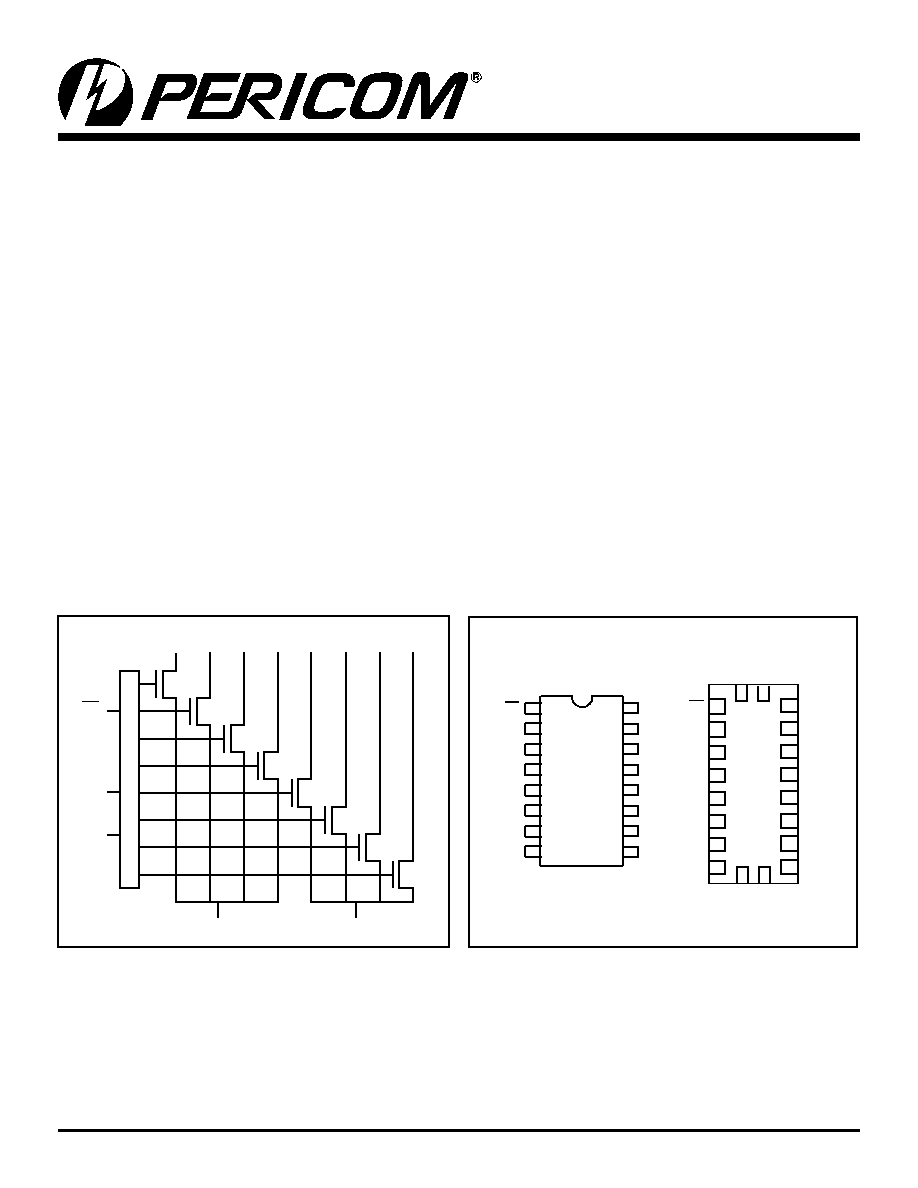
PI3CH281
Block Diagram
IA0
EN
S0
S1
IA1 IA2 IA3 IB0 IB1 IB2 IB3
YA
YB
Pin Configuration
1
2
3
4
5
16
6
15
7
14
8
13
12
11
10
9
EN
S1
IA3
IA2
IA1
IA0
YA
GND
VCC
N.C.
S0
IB3
IB2
IB1
IB0
YB
16-pin
L, Q
20-Contact
ZH
N.C.
N.C.
S0
IB3
IB2
IB1
IB0
YB
EN
S1
IA3
IA2
IA1
IA0
YA
N.C.
GN
D
N.C.
N.C.
V
CC
19
18
17
16
15
14
13
12
1
20
10
11
2
3
4
5
6
7
8
9
Notes:
1. N.C = No internal connection
2
PS8726A 07/08/04
PI3CH281
Low Voltage, High Bandwidth, 2-Channel, 4:1
Mux/DeMux, NanoSwitch
TM
with Single Enable
Storage Temperature ................................................ ≠65∞C to +150∞C
Ambient Temperature with Power Applied ............... ≠40∞C to +85∞C
Supply Voltage to Ground Potential ........................... ≠0.5V to +4.6V
DC Input Voltage ........................................................ ≠0.5V to +6.0V
DC Output Current................................................................... 120mA
Power Dissipation ....................................................................... 0.5W
Note:
Stresses greater than those listed under MAXIMUM
RATINGS may cause permanent damage to the device. This is a
stress rating only and functional operation of the device at these
or any other conditions above those indicated in the operational
sections of this specification is not implied. Exposure to absolute
maximum rating conditions for extended periods may affect re-
liability.
Maximum Ratings
(Above which the useful life may be impaired. For user guidelines, not tested.)
DC Electrical Characteristics, 3.3V Supply
(Over the Operating Range, T
A
= ≠40∞C to +85∞C, V
CC
= 3.3V ±10%)
Parameters
Description
Test Conditions
(1)
Min.
Typ
(2)
Max.
Units
V
IH
Input HIGH Voltage
Guaranteed Logic HIGH Level
2.0
V
V
IL
Input LOW Voltage
Guaranteed Logic LOW Level
≠0.5
0.8
V
IK
Clamp Diode Voltage
V
CC
= Min., I
IN
= ≠18 mA
-1.3
≠1.8
I
IH
Input HIGH Current
V
CC
= Max., V
IN
= V
CC
±1
µA
I
IL
Input LOW Current
V
CC
= Max., V
IN
= GND
±1
I
OZH
High Impedance Output Current 0 Y, In V
CC
±1
R
ON
Switch On-Resistance
(4)
V
CC
= Min., V
IN
= 0.0V,
I
ON
= 48 mA or -64mA
4
6
V
CC
= Min., V
IN
= 3.6V, I
ON
= -15 mA
5
8
Pin Description
Pin Name
Description
IA
N
, IB
N
Data Inputs
S0-1
Select Inputs
EN
Enable
YA to YB
Data Outputs
GND
Ground
V
CC
Power
Truth Table
(1)
Enable
Select
EN
S1
S0
Y
Function
H
X
X
Hi-Z
Disable
L
L
L
I0
S1-0 = 0
L
L
H
I1
S1-0 = 1
L
H
L
I2
S1-0 = 2
L
H
H
I3
S1-0 = 3
Notes:
1. H=High Voltage Level; L=Low Voltage Level

3
PS8726A 07/08/04
PI3CH281
Low Voltage, High Bandwidth, 2-Channel, 4:1
Mux/DeMux, NanoSwitch
TM
with Single Enable
Notes:
1. For Max. or Min. conditions, use appropriate value specified under Electrical Characteristics for the applicable device.
2. Typical values are at V
CC
= 3.3V, +25∞C ambient.
Notes:
1. For Max. or Min. conditions, use appropriate value specified under Electrical Characteristics for the applicable device type.
2. Typical values are at V
CC
= 3.3V, T
A
= 25∞C ambient and maximum loading.
3. Not more than one output should be shorted at one time. Duration of the test should not exceed one second.
4. Measured by the voltage drop between Y and In pin at indicated current through the switch. On-Resistance is determined
by the lower of the voltages on the two (Y, In) pins.
5. This parameter is determined by device characterization but is not production tested.
Capacitance
(T
A
= 25∞C f = 1 MHz)
Parameters
(5)
Description
Test Conditions
Typ.
Units
C
IN
Input Capacitance
V
IN
= 0V
3.0
pF
C
OFF(IN)
In Capacitance, Switch Off
3.5
C
OFF(Y)
Y Capacitance, Switch Off
12
C
ON
Y/In Capacitance, Switch On
15.0
Power Supply Characteristics
Parameters
Description
Test Conditions
(1)
Min. Typ.
(2)
Max.
Units
I
CC
Quiescent Power Supply Current
V
CC
= 3.6V, V
IN
= GND or V
CC
0.8
mA
DC Electrical Characteristics, 2.5V Supply
(Over Operating Range, T
A
= ≠40∞C to +85∞C, V
CC
= 2.5V ± 10%)
Parameters
(5)
Description
Test Conditions
Min.
Typ.
Max.
Units
V
IH
Input HIGH Voltage
Guaranteed Logic HIGH Level
1.8
≠
V
CC
+ 0.3
V
V
IL
Inout LOW Voltage
Guaranteed Logic LOW Level
≠0.3
≠
0.8
V
IK
Clamp Diode Voltage
V
CC
= Max., I
IN
= ≠6mA
≠
≠0.7
≠1.8
I
IH
Input HIGH Current
V
CC
= Max., V
IN
= V
CC
≠
≠
±1
µA
IIL
Input LOW Current
V
CC
= Max., V
IN
= GND
≠
≠
±1
I
OZH
High Impedance Current
(3)
0 Y, In V
CC
≠
≠
±1
R
ON
Switch On-Resistance
(4)
V
CC
= Min., V
IN
=0.0V,
I
ON
= ≠48mA
≠
6
8
V
CC
= Min., V
IN
= 2.25V,
I
ON
= -15mA
≠
7
14

4
PS8726A 07/08/04
PI3CH281
Low Voltage, High Bandwidth, 2-Channel, 4:1
Mux/DeMux, NanoSwitch
TM
with Single Enable
Notes:
1. See test circuit and waveforms.
2. This parameter is guaranteed but not tested on Propagation Delays.
3. The switch contributes no propagational delay other than the RC delay of the On-Resistance of the switch and the load
capacitance. The time constant for the switch alone is of the order of 0.30ns for 10pF load. Since this time constant is much
smaller than the rise/fall times of typical driving signals, it adds very little propagational delay to the system. Propagational
delay of the switch when used in a system is determined by the driving circuit on the driving side of the switch and its
interaction with the load on the driven side.
Switching Characteristics over 3.3V Operating Range
Parameters
Description
Conditions
(1)
Com.
Units
Min.
Typ.
Max.
t
PLH
t
PHL
Propogation Delay
(2,3)
Y to In, In to Y
See Test Diagram
0.3
ns
t
PZH
t
PZL
Enable Time S or EN to Y or In
See Test Diagram
1.5
9.0
t
PHZ
t
PLZ
Disable Time S or EN to Y or In
1.5
9.0
Switching Characteristics over 2.5V Operating Range
Parameters
Description
Conditions
(1)
Com.
Units
Min.
Max.
t
PLH
t
PHL
Propogation Delay
(2,3)
Y to In, In to Y
See Test Diagram
0.3
ns
t
PZH
t
PZL
Enable Time S or EN to Y or In
See Test Diagram
1.5
15.0
t
PHZ
t
PLZ
Disable Time S or EN to Y or In
1.5
12.0
Dynamic Electrical Characteristics Over the Operating Range (T
A
= -40∫ to +85∫, V
CC
= 3.3V ± 10%)
Parameter
Description
Test Condition
Min.
Typ.
Max.
Units
X
TALK
Crosstalk
See Test Diagram
-60
dB
O
IRR
Off-Isolation
See Test Diagram
-60
BW
-3dB Bandwidth
See Test Diagram
200
300
MHz
5
PS8726A 07/08/04
PI3CH281
Low Voltage, High Bandwidth, 2-Channel, 4:1
Mux/DeMux, NanoSwitch
TM
with Single Enable
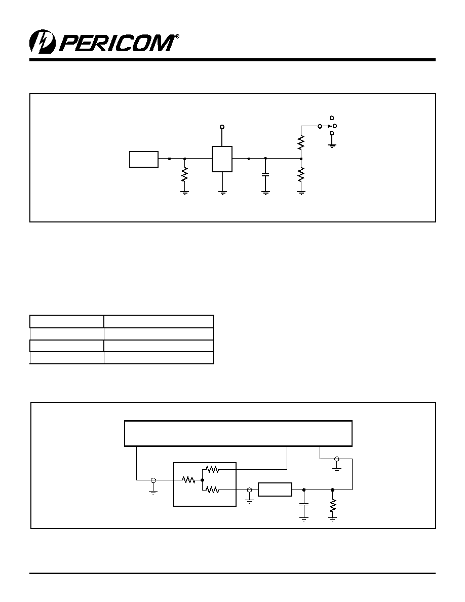
Test Circuit for Electrical Characteristics
(1)
Notes:
1. C
L
= Load capacitance: includes jig and probe capacitance.
2. R
T
= Termination resistance: should be equal to Z
OUT
of the Pulse Generator
3. Waveform 1 is for an output with internal conditions such that the output is low except when disabled by the output control.
Waveform 2 is for an output with internal conditions such that the output is high except when disabled by the output control.
4. All input impulses are supplied by generators having the following characteristics: PRR MHz, Z
O
= 50, t
R
2.5ns, t
F
2.5ns.
5. The outputs are measured one at a time with one transition per measurement.
Test Circuit for Dynamic Electrical Characteristics
RT
10pF
CL
VCC
VIN
VOUT
200
200
6.0V
Pulse
Generator
D.U.T
V
CC
D.U.T
T1
R1
S1
HP11667A
50
10
pF
HP4195A
Switch Positions
Test
Switch
t
PLZ
, t
PZL
6.0V
t
PHZ
, t
PZH
GND
Prop Delay
Open