 | –≠–ª–µ–∫—Ç—Ä–æ–Ω–Ω—ã–π –∫–æ–º–ø–æ–Ω–µ–Ω—Ç: PI3USB40A | –°–∫–∞—á–∞—Ç—å:  PDF PDF  ZIP ZIP |

1
PS8698A 02/01/05
Features
∑ R
ON
is 4 typical
∑ Low bit-to-bit skew: 200ps
∑ Low crosstalk: ≠27dB @ 250MHz
∑ Low Current Consumption; 20A
∑ Near-Zero propagation delay: 250ps
∑ Switching speed: 3ns
∑ Channel On-Capacitance: 6pF (typical)
∑ V
CC
Operating Range: +3.0V to +3.6V
∑ ESD >2000V . . . Human Body Model
∑ >500MHz bandwidth (or data frequency)
∑ Packaging (Pb-free & Green available):
-48-pin 240 mil wide plastic TSSOP (A)
Applications
∑ Routes physical layer signals for high-speed, high
bandwidth differential protocols
Description
The PI3USB40 is a 16- to 8-channel multiplexer/demultiplexer
Switch with Hi-Z outputs. Industry leading advantages include
a propagation delay of less than 250ps, resulting from its low
channel resistance and I/O capacitance. The device multiplexes
differential outputs from a USB transceiver device to one of two
corresponding outputs.
The switch is bidirectional and offers little or no attenuation of the
high-speed signals at the outputs. It is designed for low bit-to-bit
skew, high channel-to-channel noise isolation and is compatible
with various standards, such as High Speed USB 2.0 (480 Mb/s).
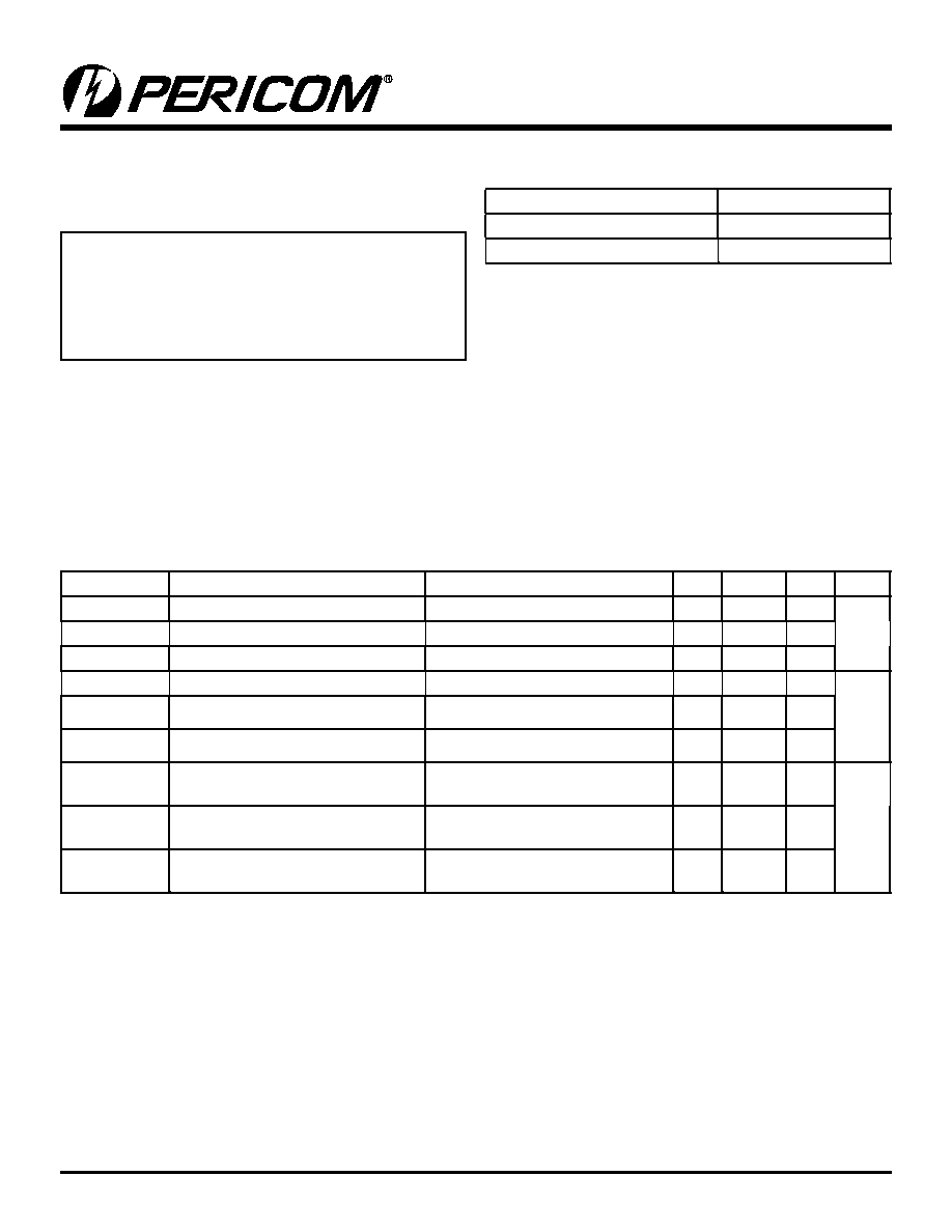
Block Diagram
Pin Description
PI3USB40
3.3V, Wide Bandwidth, 8-Channel,
2:1 Mux/DeMux USB 2.0 Switch with Single Enable
Y
0
Y
1
0
I
1
1
I
1
0
I
2
1
I
2
2
I
1
3
I
1
2
I
2
3
I
2
4
I
1
5
I
1
4
I
2
5
I
2
6
I
1
7
I
1
6
I
2
7
I
2
Y
2
Y
3
Y
4
Y
5
Y
6
Y
7
1
0I
1
1
I
1
GND
0I
2
1
I
2
GND
2
I
1
3
I
1
GND
2
I
2
3
I
2
GND
V
DD
4
I
1
5
I
1
GND
4
I
2
5
I
2
GND
6
I
1
7
I
1
GND
6
I
2
7
I
2
V
DD
Y
0
GND
Y
1
GND
V
DD
GND
Y
2
GND
Y
3
GND
V
DD
GND
NC
Y
4
GND
Y
5
GND
V
DD
GND
Y
6
GND
Y
7
SEL
2
3
4
5
6
7
8
9
10
11
12
13
14
15
16
17
18
19
38
37
36
35
34
48
47
46
45
44
43
33
32
31
30
42
41
40
39
20
21
22
23
24
29
28
27
26
25
2
PS8698A 02/01/05
PI3USB40
3.3V, Wide Bandwidth, 8-Channel,
2:1, Mux/DeMux USB 2.0 Switch with Single Enable
Storage Temperature....................................≠65∞C to +150∞C
Supply Voltage to Ground Potential...............≠0.5V to +4.0V
DC Input Voltage............................................≠0.5V to +5.5V
DC Output Current......................................................120mA
Power Dissipation...........................................................0.5W
Note:
Stresses greater than those listed under MAXIMUM RATINGS may cause
permanent damage to the device. This is a stress rating only and func-
tional operation of the device at these or any other conditions above those
indicated in the operational sections of this specification is not implied.
Exposure to absolute maximum rating conditions for extended periods
may affect reliability.
Maximum Ratings
(Above which useful life may be impaired. For user guidelines,
not tested.)
Truth Table
Function
SEL
Y
N
to
N
I
1
L
Y
N
to
N
I
2
H
DC Electrical Characteristics for USB 2.0 Switching over Operating Range
(T
A
= ≠40∞C to +85∞C, V
CC
= 3.3V ±10%)
Paramenter
Description
Test Conditions
Min. Typ.
(2)
Max. Units
V
IH
Input HIGH Voltage
Guaranteed HIGH level
2
V
V
IL
Input LOW Voltage
Guaranteed LOW level
0.8
V
IK
Clamp Diode Voltage
V
CC
= Max., I
IN
= ≠18mA
≠0.7
≠1.2
I
IH
Input HIGH Current
V
CC
= Max., V
IN
= V
CC
±5
µA
I
IL
Input LOW Current
V
CC
= Max., V
IN
= GND
±5
I
OFF
Power Down Leakage Current
V
CC
= 0V, V
A
= 0V, V
B
3.6
R
ON
Switch On-Resistance(3)
V
CC
= Min., 1.5V V
IN
V
CC,
I
IN
= ≠40mA
4
8
R
FLAT(ON)
On-Resistance Flatness(4)
V
CC
= Min., V
IN
@ 1.5V and V
CC
,
I
IN
= ≠40mA
1
R
ON
On-Resistance match from center
ports to any other port(4)
V
CC
= Min., 1.5V V
IN
V
CC
,
I
IN
= ≠40mA
0.9
2
3
PS8698A 02/01/05
PI3USB40
3.3V, Wide Bandwidth, 8-Channel,
2:1, Mux/DeMux USB 2.0 Switch with Single Enable
Notes:
1. For max. or min. conditions, use appropriate value specified under Electrical Characteristics for the applicable device type.
2. Typical values are at V
CC
= 3.3V, T
A
= 25∞C ambient and maximum loading.
3. Per TTL driven input (control inputs only); A and B pins do not contribute to I
CC
.
Dynamic Electrical Characteristics Over the Operating Range
(TA=-40∫ to +85∫C, VCC=3.3V±10%, GND=0V)
Parameter
Description
Test Conditions
Min.
Typ.
(2)
Max.
Units
X
TALK
Crosstalk
R
L
= 100, f = 250MHz
-27
dB
O
IRR
OFF Isolation
-32
BW
Bandwidth ≠3dB
R
L
= 100
500
MHz
Notes:
1. For Max. or Min. conditions, use appropriate value specified under Electrical Characteristics for the applicable device type.
2. Guaranteed by design.
3. The bus switch contributes no propagational delay other than the RC delay of the On-Resistance of the switch and the load capacitance. The
time constant for the switch alone is of the order of 0.25ns for 10pF load. Since this time constant is much smaller than the rise/fall times of
typical driving signals, it adds very little propagational delay to the system. Propagational delay of the bus switch when used in a system is
determined by the driving circuit on the driving side of the switch and its interactions with the load on the driven side.
Power Supply Characteristics
Parameters
Description
Test Conditions
(1)
Min.
Typ.
(2)
Max.
Units
I
CC
Quiescent Power Supply Current
V
CC
= Max., V
IN
= GND or V
CC
800
µA
Notes:
1. For max. or min. conditions, use appropriate value specified under Electrical Characteristics for the applicable device type.
2. Typical values are at V
CC
= 3.3V, T
A
= 25∞C ambient and maximum loading.
3. Measured by the voltage drop between A and B pins at indicated current through the switch. On-Resistance is determined by the lower of the
voltages on the two (A & B) pins.
4. This parameter is determined by device characterization but is not production tested.
Capacitance
(T
A
= 25∞C, f = 1MHz)
Parameters
(5)
Description
Test Conditions
Typ.
Max.
Units
C
IN
Input Capacitance
V
IN
= 0V
2.0
3.0
pF
C
OFF
Port I Capacitance, Switch OFF
4.0
6.0
C
ON
Switch Capacitance, Switch ON
6.0
10.0
Switching Characteristics
Paramenter
Description
Test
Conditions Min. Typ.
(2)
Max. Units
tPD
Propagation Delay(2,3)
0.25
ns
tPZH, tPZL Line Enable Time - SEL to YN, IN
0.5
15
tPHZ, tPLZ Line Disable Time - SEL to YN, IN
0.5
9
tSK(o)
Output Skew between center port (Y4 to Y5) to any other port(2)
0.1
0.2
tSK(p)
Skew between opposite transitions of the same output (tPHL
- tPLH) (2)
0.1
0.2

4
PS8698A 02/01/05
PI3USB40
3.3V, Wide Bandwidth, 8-Channel,
2:1, Mux/DeMux USB 2.0 Switch with Single Enable
Test Circuit for Electrical Characteristics
(1)
Notes:
1. C
L
= Load capacitance: includes jig and probe capacitance.
2. R
T
= Termination resistance: should be equal to Z
OUT
of the Pulse Generator
3. Waveform 1 is for an output with internal conditions such that the output is low except when disabled by the output control.
Waveform 2 is for an output with internal conditions such that the output is high except when disabled by the output control.
4. All input impulses are supplied by generators having the following characteristics: PRR MHz, Z
O
= 50, t
R
2.5ns, t
F
2.5ns.
5. The outputs are measured one at a time with one transition per measurement.
Test Circuit for Dynamic Electrical Characteristics
Switch Positions
Test
Switch
t
PLZ
, t
PZL
(output on B-side)
6.0V
t
PHZ
, t
PZH
(output on B-side)
GND
Prop Delay
Open
RT
10pF
C
L
V
CC
V
IN
V
OUT
200-ohm
200-ohm
6.0V
Pulse
Generator
D.U.T
V
CC
PI3USB40
T1
R1
S1
HP11667A
50-ohm
10pF
HP4195A

5
PS8698A 02/01/05
PI3USB40
3.3V, Wide Bandwidth, 8-Channel,
2:1, Mux/DeMux USB 2.0 Switch with Single Enable
Voltage Waveforms Propagation Delay Times
Switching Waveforms
Output Skew - t
SK(o)
Pulse Skew - t
SK(p)
Voltage Waveforms Enable and Disable Times
Data In
Data Out
at Channel X
Data Out
at Channel Y
t
PLHX
t
PHLX
3.5V
2.5V
2.5V
2.5V
I
t
SK(o)
= I t
PLHy
≠ t
PLHx
I or I t
PHLy
≠ t
PHLx
I
t
SK(o)
t
PLHy
t
PHLy
V
OH
V
OL
V
OL
V
OH
1.5V
Input
Output
t
PLH
t
SK(p)
= I t
PHL
≠ t
PLH
I
t
PHL
3.5V
2.5V
2.5V
V
OL
V
OH
1.5V
Applications Information
Logic Inputs
The logic control inputs can be driven up to +3.6V regardless of the supply voltage. For example, given a +3.3V supply, the output
enables or select pins may be driven low to 0V and high to 3.6V. Driving IN Rail-to-RailÆ minimizes power consumption.
Power-Supply Sequencing
Proper power-supply sequencing is advised for all CMOS devices. It is recommended to always apply V
CC
before applying signals to
the input/output or control pins.
Rail-to-Rail is a registered trademark of Nippon Motorola, Ltd
Input
t
PLH
2.5V
2.5V
2.5V
2.5V
t
PHL
3.5V
1.5V
Output
V
OH
V
OL
tPLZ
1.25V
1.25V
2.5V
V
OH
0V
V
OL
V
DD/2
V
DD/2
t
PHZ
t
PZL
t
PZH
Output
Output
V
OL
+0.3V
V
OH
≠0.3V
V
OL
V
OH
SEL