1
PS8560A 09/27/04
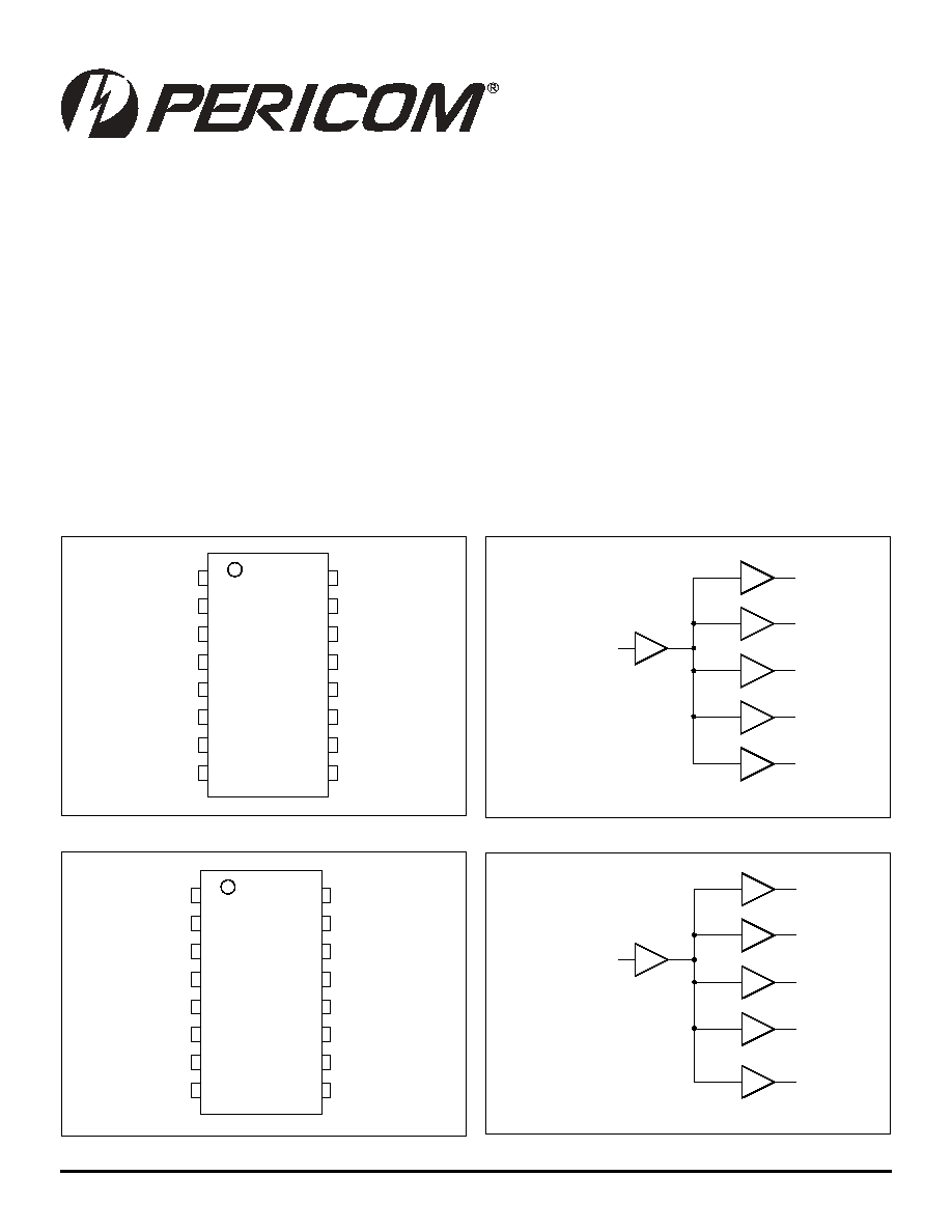
Pin Configuration (PI49FCT20802)
Features
∑ High Frequency >150 MHz
∑ High-speed, low-noise, non-inverting clock buffer
≠ PI49FCT20802 is a 1:5 buffer
≠ PI49FCT20803 is a 1:7 buffer
∑ Low skew < 150ps
∑ Low duty cycle distortion < 300ps
∑ Low propagation delay < 3.5ns
∑ Multiple V
DD
, GND pins for noise reduction
∑ 2.5V supply voltage and 3V tolerant input
∑ Packages:
- 16-pin TSSOP (L)
- 16-pin QSOP (Q)
12345678901234567890123456789012123456789012345678901234567890121234567890123456789012345678901212345678901234567890123456789012123456789012
12345678901234567890123456789012123456789012345678901234567890121234567890123456789012345678901212345678901234567890123456789012123456789012
1:5/1:7 2.5V Clock Buffer for
Networking Applications
PI49FCT20802/
PI49FCT20803
Description
The PI49FCT2080x is 2.5V, high-speed, low noise, non-inverting
clock buffer. It is designed to target networking applications that
require low-skew, low-jitter, and high-frequency clock distribution.
It provides output-to-output skew as low as 150ps, and is an ideal
clock distribution device for synchronous systems. PI49FCT2080x
is a clock buffer from a single input that produces five outputs
on PI49FCT20802 and seven outputs on PI49FCT20803.
PI49FCT2080x is characterized for operation from ≠40
∞
C to 85
∞
C.
1
2
3
VDD
4
CLK1
5
CLK0
6
NC
7
VDD
8
GND
VDD
CLK3
GND
VDD
NC
GND
16
15
14
13
12
11
10
9
BUF_IN
GND
CLK2
CLK4
CLK4
CLK2
CLK1
CLK0
BUF_IN
CLK3
Pin Configuration (PI49FCT20803)
1
2
3
VDD
4
CLK1
5
CLK0
6
CLK2
7
VDD
8
GND
VDD
CLK5
GND
VDD
CLK3
GND
16
15
14
13
12
11
10
9
BUF_IN
GND
CLK4
CLK6
CLK6
CLK2
CLK1
CLK0
BUF_IN
CLK3
. . .
Block Diagram (PI49FCT20802)
Block Diagram (PI49FCT20803)

2
PS8560A 09/27/04
12345678901234567890123456789012123456789012345678901234567890121234567890123456789012345678901212345678901234567890123456789012123456789012
12345678901234567890123456789012123456789012345678901234567890121234567890123456789012345678901212345678901234567890123456789012123456789012
PI49FCT20802/PI49FCT20803
1:5/1:7 2.5V Clock Buffer for
Networking Applications
Storage Temperature .....................................≠65∞C to +150∞C
Supply Voltage V
DD ..................................................
≠0.5V to +3.6V
Input/Output Voltages
(1) ................................
≠0.5V to V
DD
+0.5V
DC Output Current ...................................... ≠60mA to +60mA
Power Dissipation ....................................................... 500mW
Maximum Ratings
(Above which the useful life may be impaired. For user guidelines, not tested.)
Note:
Stresses greater than those listed under MAXIMUM RATINGS
may cause permanent damage to the device. This is a stress rating
only and functional operation of the device at these or any other
conditions above those indicated in the operational sections of this
specification is not implied. Exposure to absolute maximum rating
conditions for extended periods may affect reliability.
Notes:
1. This value is limited to 3.6V maximum.
2. For Max. or Min. conditions, use appropriate value specified under Electrical Characteristics for the applicable device type.
3. Typical values are at V
DD
= 2.5V, +25∞C ambient and maximum loading.
s
r
e
t
e
m
a
r
a
P
n
o
i
t
p
i
r
c
s
e
D
s
n
o
i
t
i
d
n
o
C
t
s
e
T
)
2
(
.
n
i
M
.
p
y
T
)
3
(
.
x
a
M
s
t
i
n
U
V
H
I
e
g
a
tl
o
V
H
G
I
H
t
u
p
n
I
7
.
1
V
V
L
I
e
g
a
tl
o
V
W
O
L
t
u
p
n
I
7
.
0
I
I
t
n
e
r
r
u
C
t
u
p
n
I
V
D
D
V
r
o
0
=
D
D
1
±
mA
V
K
I
e
g
a
tl
o
V
e
d
o
i
D
p
m
a
l
C
V
D
D
I
,.
n
i
M
=
N
I
A
m
8
1
≠
=
7
.
0
≠
1
≠
V
V
H
O
H
G
I
H
t
u
p
t
u
O
e
g
a
tl
o
V
V
D
D
.
n
i
M
=
I
H
O
A
m
1
≠
=
2
I
H
O
A
m
8
≠
=
8
.
1
)
3
(
V
L
O
e
g
a
tl
o
V
W
O
L
t
u
p
t
u
O
V
D
D
.
n
i
M
=
I
L
O
A
m
1
=
4
.
0
I
L
O
A
m
8
=
6
.
0
DC Electrical Characteristics
(Over the Operating Range)
Operating Range
V
DD
Voltage ........................................................... 2.5V ± 0.2V
Industrial Temperature .................................... ≠40∞C to +85∞C
Commercial Temperature ..................................... 0∞C to +70∞C
Capacitive Loading ............................................. 10pF to 25pF

3
PS8560A 09/27/04
12345678901234567890123456789012123456789012345678901234567890121234567890123456789012345678901212345678901234567890123456789012123456789012
12345678901234567890123456789012123456789012345678901234567890121234567890123456789012345678901212345678901234567890123456789012123456789012
PI49FCT20802/PI49FCT20803
1:5/1:7 2.5V Clock Buffer for
Networking Applications
Notes:
4. For Max. or Min. conditions, use appropriate value specified under Electrical Characteristics for the applicable device.
5. Typical values are at V
DD
= 2.5V, +25∞C ambient and maximum loading.
6. Per TTL driven input (V
IN
= V
DD
≠ 0.6V); all other inputs at V
DD
or GND.
Capacitance
(T
A
= 25∞C, f = 1 MHz)
Note:
7. This parameter is determined by device characterization but is not production tested.
s
r
e
t
e
m
a
r
a
P
n
o
i
t
p
i
r
c
s
e
D
s
n
o
i
t
i
d
n
o
C
t
s
e
T
)
4
(
.
n
i
M
.
p
y
T
)
5
(
.
x
a
M
s
t
i
n
U
I
Q
D
D
t
n
e
r
r
u
C
y
l
p
p
u
S
r
e
w
o
P
t
n
e
c
s
e
i
u
Q
V
N
I
V
r
o
0
=
D
D
1
.
0
0
2
A
µ
I
D
D
s
t
u
p
n
I
r
e
p
t
n
e
r
r
u
C
y
l
p
p
u
S
V
N
I
V
=
D
D
V
6
.
0
≠
)
6
(
7
4
0
0
3
I
D
D
)
1
h
p
a
r
G
e
e
S
(
t
n
e
r
r
u
C
y
l
p
p
u
S
c
i
m
a
n
y
D
V
D
D
,
d
a
o
l
m
h
o
-
3
3
&
F
p
5
1
,
V
7
.
2
=
z
H
M
0
5
1
=
f
6
3
1
A
m
Power Supply Characteristics
Graph 1. Dynamic Current vs. Clock Frequency
160
140
120
100
80
60
Clock Frequency [MHz]
Dynamic Current - I
DD
[mA]
40
20
0
0
50
100
150
200
Load = 15pF & 33 ohms
Load = 0
s
r
e
t
e
m
a
r
a
P
n
o
i
t
p
i
r
c
s
e
D
s
n
o
i
t
i
d
n
o
C
t
s
e
T
p
y
T
)
7
(
.
x
a
M
s
t
i
n
U
C
N
I
e
c
n
a
ti
c
a
p
a
C
t
u
p
n
I
V
N
I
V
0
=
3
4
F
p
C
T
U
O
e
c
n
a
ti
c
a
p
a
C
t
u
p
t
u
O
V
T
U
O
V
0
=
6
4
PS8560A 09/27/04
12345678901234567890123456789012123456789012345678901234567890121234567890123456789012345678901212345678901234567890123456789012123456789012
12345678901234567890123456789012123456789012345678901234567890121234567890123456789012345678901212345678901234567890123456789012123456789012
PI49FCT20802/PI49FCT20803
1:5/1:7 2.5V Clock Buffer for
Networking Applications
Notes:
8. See test circuit and waveforms.
9. Identical conditions: loading, transitions, supply voltage, temperature, package type and speed grade.
s
r
e
t
e
m
a
r
a
P
n
o
i
t
p
i
r
c
s
e
D
s
n
o
i
t
i
d
n
o
C
t
s
e
T
)
8
(
.
n
i
M
.
p
y
T
.
x
a
M
s
t
i
n
U
f
K
L
C
y
c
n
e
u
q
e
r
F
t
u
p
t
u
O
0
5
1
z
H
M
t
R
t/
F
V
e
m
it
ll
a
F
/
e
s
i
R
O
V
7
.
1
~
V
7
.
0
=
C
L
z
H
M
0
0
1
,
F
p
2
2
=
0
.
1
5
2
.
1
s
n
C
L
z
H
M
0
5
1
,
F
p
2
1
=
0
.
1
2
.
1
t
D
P
y
a
l
e
D
n
o
it
a
g
a
p
o
r
P
C
L
z
H
M
0
0
1
,
F
p
2
2
=
5
.
3
5
.
3
C
L
z
H
M
0
5
1
,
F
p
2
1
=
4
.
2
7
.
2
t
)
o
(
K
S
w
e
k
S
t
u
p
t
u
O
C
L
z
H
M
0
0
1
,
F
p
2
2
=
0
0
1
0
5
1
s
p
C
L
z
H
M
0
5
1
,
F
p
2
1
=
0
0
1
0
5
1
t
)
p
(
K
S
w
e
k
S
e
s
l
u
P
C
L
z
H
M
0
0
1
,
F
p
2
2
=
0
5
2
0
0
3
C
L
z
H
M
0
5
1
,
F
p
2
1
=
0
5
2
0
0
3
t
)
d
(
K
S
w
e
k
s
e
c
i
v
e
d
-
o
t
-
e
c
i
v
e
D
)
9
(
C
L
z
H
M
0
5
1
,
F
p
2
1
=
0
0
4
0
0
6
Switching Characteristics
(V
DD
= 2.5V ± 0.2V, T
A
= 85∞C)
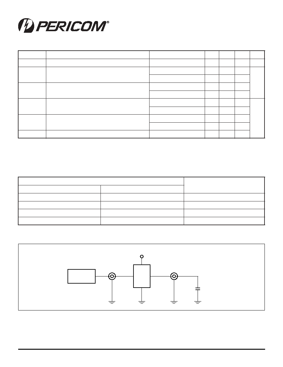
Test Circuits for All Outputs
Pulse
Generator
D.U.T.
V
IN
V
OUT
C
L
V
DD
e
m
a
N
n
i
P
n
o
i
t
p
i
r
c
s
e
D
2
0
8
0
2
T
C
F
9
4
I
P
3
0
8
0
2
T
C
F
9
4
I
P
N
I
_
F
U
B
N
I
_
F
U
B
t
u
p
n
I
]
4
:
0
[
K
L
C
]
6
:
0
[
K
L
C
s
t
u
p
t
u
O
D
N
G
D
N
G
D
N
G
V
D
D
V
D
D
r
e
w
o
P
Product Pin Description
5
PS8560A 09/27/04
12345678901234567890123456789012123456789012345678901234567890121234567890123456789012345678901212345678901234567890123456789012123456789012
12345678901234567890123456789012123456789012345678901234567890121234567890123456789012345678901212345678901234567890123456789012123456789012
PI49FCT20802/PI49FCT20803
1:5/1:7 2.5V Clock Buffer for
Networking Applications
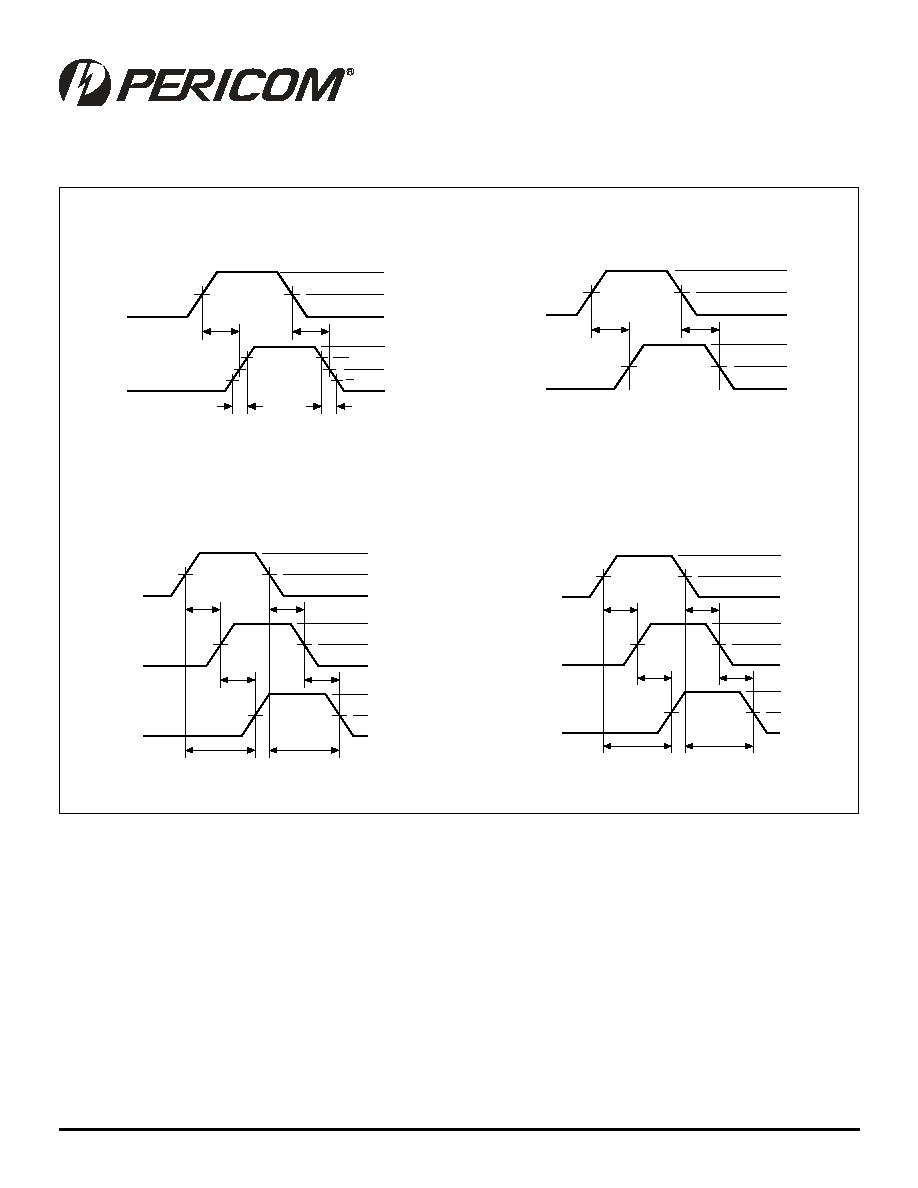
Switching Waveforms
Propagation Delay
Package Skew ≠ t
SK(T)
Pulse Skew ≠ t
SK(P)
Output Skew ≠ t
SK(O)
Input
t
PLHx
3V
1.5V
0V
CLKx
V
OH
1.5V
V
OL
t
PHLx
t
SK(o)
CLKy
V
OH
1.5V
V
OL
t
SK(o)
t
PLHy
t
PHLy
t
SK(o)
=
t
PLHy
≠ t
PLHx
or
t
PHLy
≠ t
PHLx
Input
t
PLH1
3V
1.5V
0V
Package 1
Output
V
OH
1.5V
V
OL
t
PHL1
t
SK(t)
Package 2
Output
V
OH
1.5V
V
OL
t
SK(t)
t
PLH2
t
PHL2
t
SK(t)
=
t
PLH2
≠ t
PLH1
or
t
PHL2
≠ t
PHL1
Input
t
PLH
3V
1.25V
0V
Output
V
OH
1.25V
V
OL
t
PHL
2.0V
0.6V
t
R
t
F
Input
t
PLH
3V
1.5V
0V
Output
V
OH
1.5V
V
OL
t
PHL
t
SK(p)
= | t
PHL
≠ t
PLH
|