1
PS8493 08/09/00
1
2
3
VDD
4
CLK1
5
CLK0
6
CLK2
7
VDD
8
GND
9
GND
10
VDD
CLK8
GND
VDD
CLK6
GND
CLK5
20
CLK4
19
18
17
16
15
14
13
12
11
BUF_IN
GND
CLK3
CLK7
CLK9
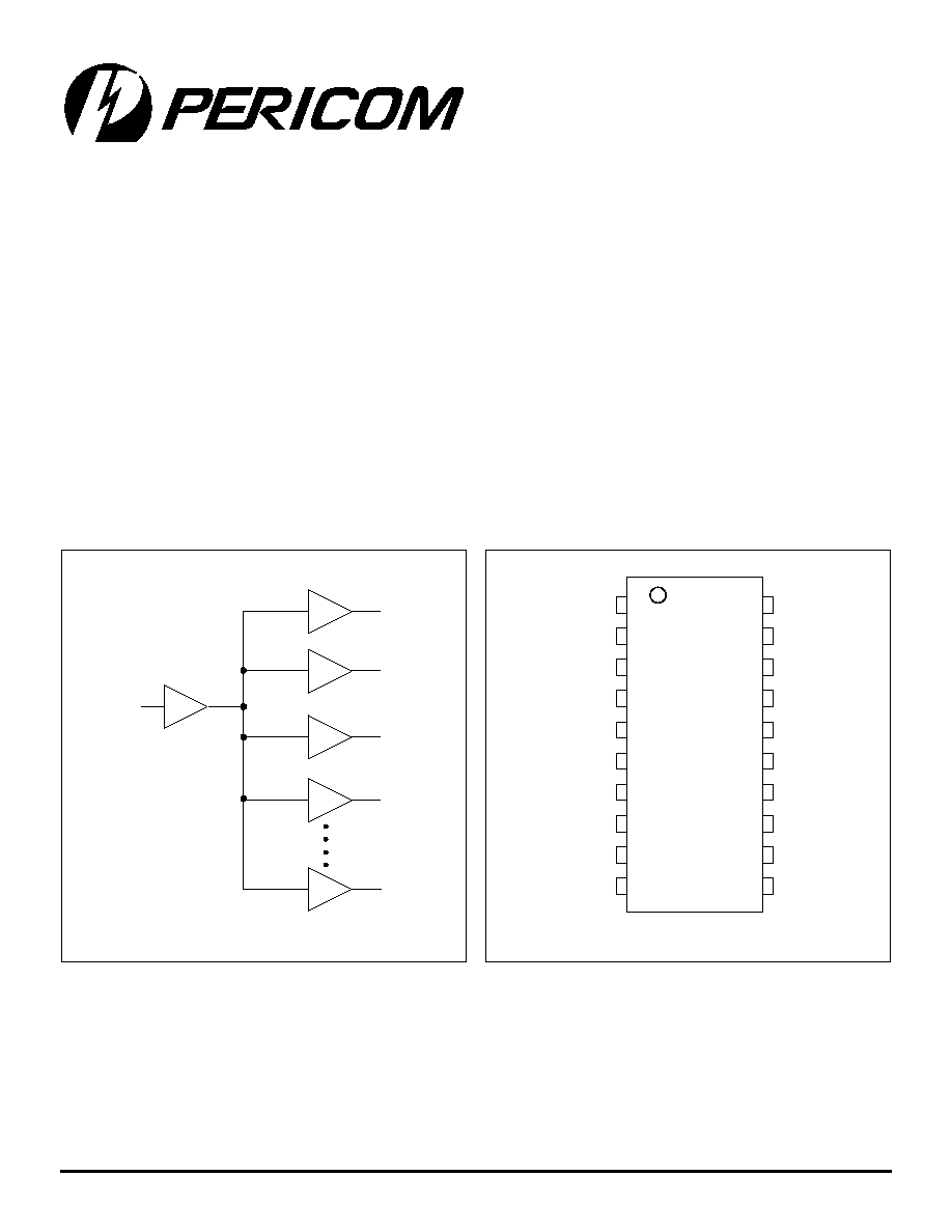
Pin Configuration
Block Diagram
Product Features
High Frequency >156 MHz
High-speed, low-noise, non-inverting 1-10 buffer
Low-skew (<250ps) between any two output clocks
Low duty cycle distortion <250ps
Low propagation delay <2.5ns
Multiple V
DD
, GND pins for noise reduction
3.3V supply voltage
Available in SOIC, SSOP, and QSOP packages
12345678901234567890123456789012123456789012345678901234567890121234567890123456789012345678901212345678901234567890123456789012123456789012
12345678901234567890123456789012123456789012345678901234567890121234567890123456789012345678901212345678901234567890123456789012123456789012
1-10 Clock Buffer for Networking Applications
PI49FCT3807D
20-Pin
H,Q,S
Description
The PI49FCT3807D is a 3.3V compatible, high-speed, low-noise
1-10 non-inverting clock buffer. The key goal in designing the
PI6C3807D is to target networking applications that require low-
skew, low-jitter, and high-frequency clock distribution. Providing
output-to-output skew as low as 150ps, the PI49FCT3807D is an
ideal clock distribution device for synchronous systems. Design-
ing synchronous networking systems requires a tight level of skew
from a large number of outputs.
CLK9
CLK2
CLK1
CLK0
BUF_IN
CLK3
2
PS8493 08/09/00
12345678901234567890123456789012123456789012345678901234567890121234567890123456789012345678901212345678901234567890123456789012123456789012
12345678901234567890123456789012123456789012345678901234567890121234567890123456789012345678901212345678901234567890123456789012123456789012
PI49FCT3807D
1-10 Clock Buffer for Networking Applications
Storage Temperature ........................................................... 65�C to +150�C
V
DD
Voltage ........................................................................... 0.5V to +4.6V
Output Voltage ................................................................ 0.5V to V
DD
+0.5V
Input Voltage ......................................................................... 0.5V to +7.0V
DC Output Current .............................................................60mA to +60mA
Power Dissipation ............................................................................. 500mW
Maximum Ratings
(Above which the useful life may be impaired. For user guidelines, not tested.)
Note:
Stresses greater than those listed under MAXIMUM
RATINGS may cause permanent damage to the
device. This is a stress rating only and functional
operation of the device at these or any other condi-
tions above those indicated in the operational sec-
tions of this specification is not implied. Exposure to
absolute maximum rating conditions for extended
periods may affect reliability.
Notes:
1. For Max. or Min. conditions, use appropriate value specified under Electrical Characteristics for the applicable device type.
2. Typical values are at V
CC
= 3.3V, +25�C ambient and maximum loading.
3. V
OH
= V
CC
0.6V at rated current.
4. This parameter is determined by device characterization but is not production tested.
5. Not more than one output should be shorted at one time. Duration of the test should not exceed one second.
s
r
e
t
e
m
a
r
a
P
n
o
it
p
i
r
c
s
e
D
s
n
o
it
i
d
n
o
C
t
s
e
T
)
1
(
.
n
i
M
.
p
y
T
)
2
(
.
x
a
M
s
ti
n
U
V
H
I
e
g
a
tl
o
V
H
G
I
H
t
u
p
n
I
)
s
n
i
P
t
u
p
n
I(
l
e
v
e
L
H
G
I
H
ci
g
o
L
d
e
e
t
n
a
r
a
u
G
0
.
2
5
.
5
V
V
L
I
e
g
a
tl
o
V
W
O
L
t
u
p
n
I
)
s
n
i
P
t
u
p
n
I(
l
e
v
e
L
W
O
L
ci
g
o
L
d
e
e
t
n
a
r
a
u
G
5
.
0
8
.
0
I
H
I
t
n
e
rr
u
C
H
G
I
H
t
u
p
n
I
V
D
D
.
x
a
M
=
V
N
I
V
=
D
D
1
�
A
I
L
I
t
n
e
rr
u
C
W
O
L
t
u
p
n
I
V
D
D
.
x
a
M
=
V
N
I
D
N
G
=
1
V
K
I
e
g
a
tl
o
V
e
d
o
i
D
p
m
al
C
V
D
D
I
,.
n
i
M
=
N
I
A
m
8
1
=
7
.
0
2
.
1
V
V
H
O
e
g
a
tl
o
V
H
G
I
H
t
u
p
t
u
O
V
D
D
V
,.
n
i
M
=
N
I
V
=
H
I
V
r
o
L
I
I
H
O
A
m
1
.
0
=
V
D
D
2
.
0
I
H
O
A
m
2
1
=
4
.
2
)
3
(
0
.
3
V
L
O
e
g
a
tl
o
V
W
O
L
t
u
p
t
u
O
V
D
D
V
,.
n
i
M
=
N
I
V
=
H
I
V
r
o
L
I
I
L
O
A
m
1
.
0
=
2
.
0
I
L
O
A
m
2
1
=
3
.
0
5
.
0
I
H
O
t
n
e
rr
u
C
H
G
I
H
t
u
p
t
u
O
V
D
D
V
,
V
0
.
3
=
N
I
V
=
H
I
V
r
o
L
I
V
,
T
U
O
V
5
.
1
=
)
4
(
5
4
5
7
0
8
1
A
m
I
L
O
t
n
e
rr
u
C
W
O
L
t
u
p
t
u
O
V
D
D
V
,
V
0
.
3
=
N
I
V
=
H
I
V
r
o
L
I
V
,
T
U
O
V
5
.
1
=
)
4
(
0
5
2
9
0
0
2
DC Electrical Characteristics
(Over the Operating Range)
Operating Range
V
DD
Voltage ................................................................................. 3.3V � 0.3V
Commercial Temperature ......................................................... 0�C to +70�C
Industrial Temperature ............................................................. 40V to +85V
Input Frequency .................................................................... DC to 156 MHz
Capacitive Loading ................................................................... 10pF to 50pF
3
PS8493 08/09/00
12345678901234567890123456789012123456789012345678901234567890121234567890123456789012345678901212345678901234567890123456789012123456789012
12345678901234567890123456789012123456789012345678901234567890121234567890123456789012345678901212345678901234567890123456789012123456789012
PI49FCT3807D
1-10 Clock Buffer for Networking Applications
Notes:
1. For Max. or Min. conditions, use appropriate value specified under Electrical Characteristics for the applicable device.
2. Typical values are at V
DD
= 3.3V, +25�C ambient.
3. Per TTL driven input (V
IN
= V
DD
0.6V); all other inputs at V
DD
or GND.
Pin Name
Description
BUF_IN
Input
CLK [0:9]
Outputs
GND
Ground
V
DD
Power
Product Pin Description
Capacitance
(T
A
= 25�C, f = 1 MHz)
Parameters
(1)
Description
Test Conditions
Typ
Max.
Units
C
IN
Input Capacitance
V
IN
= 0V
3.0
4
C
OUT
Output Capacitance
V
OUT
= 0V
6
Note:
1. This parameter is determined by device characterization but is not production tested.
Test Circuits for All Outputs
Definitions:
C
L
= Load capacitance: includes jig and probe capacitance.
R
T
= Termination resistance, should be equal to Zout of the
Pulse Generator.
pF
s
r
e
t
e
m
a
r
a
P
n
o
it
p
i
r
c
s
e
D
s
n
o
it
i
d
n
o
C
t
s
e
T
)
1
(
.
n
i
M
.
p
y
T
)
2
(
.
x
a
M
s
ti
n
U
I
Q
D
D
t
n
e
rr
u
C
y
l
p
p
u
S
r
e
w
o
P
t
n
e
c
s
ei
u
Q
V
D
D
.
x
a
M
=
V
N
I
V
r
o
D
N
G
=
D
D
1
.
0
0
3
A
�
I
D
D
r
e
p
t
n
e
rr
u
C
y
l
p
p
u
S
H
G
I
H
L
T
T
@
st
u
p
n
I
V
D
D
.
x
a
M
=
V
N
I
V
=
D
D
V
6
.
0
)
3
(
7
4
0
0
3
I
D
D
t
n
e
rr
u
C
y
l
p
p
u
S
ci
m
a
n
y
D
V
D
D
,
V
6
.
3
=
d
a
o
L
o
N
z
H
M
0
5
3
4
A
m
z
H
M
7
6
6
5
z
H
M
0
8
6
6
z
H
M
0
0
1
1
8
z
H
M
5
2
1
7
9
z
H
M
6
5
1
1
2
1
Power Supply Characteristics
Pulse
Generator
D.U.T.
V
IN
V
OUT
CL
V
DD

4
PS8493 08/09/00
12345678901234567890123456789012123456789012345678901234567890121234567890123456789012345678901212345678901234567890123456789012123456789012
12345678901234567890123456789012123456789012345678901234567890121234567890123456789012345678901212345678901234567890123456789012123456789012
PI49FCT3807D
1-10 Clock Buffer for Networking Applications
Notes:
1. See test circuit and waveforms.
2. Minimum limits are guaranteed but not tested on Propagation Delays.
3. Skew measured at worse cast temperature (max. temp).
4. Identical conditions: loading, transitions, supply voltage, temperature, package type and speed grade.
s
r
e
t
e
m
a
r
a
P
n
o
it
p
ir
c
s
e
D
s
n
o
it
i
d
n
o
C
t
s
e
T
)
1
(
.
n
i
M
.
p
y
T
.
x
a
M
s
ti
n
U
F
t/
R
t
V
0
.
2
~
V
8
.
0
e
m
i
T
ll
a
F
/
e
si
R
n
K
L
C
C
L
z
H
M
5
2
1
,
F
p
5
1
=
7
.
0
0
.
1
s
n
t
H
L
P
t
L
H
P
n
K
L
C
o
t
N
I
_
F
U
B
y
al
e
D
n
oi
t
a
g
a
p
o
r
P
C
L
z
H
M
5
2
1
,
F
p
5
1
=
0
.
1
2
.
2
5
.
2
t
)
o
(
K
S
)
3
(
e
g
a
k
c
a
p
e
m
a
s
e
h
t
f
o
st
u
p
t
u
o
o
w
t
n
e
e
w
t
e
b
w
e
k
S
)
n
oi
ti
s
n
a
rt
e
m
a
s
(
C
L
z
H
M
5
2
1
,
F
p
5
1
=
0
1
1
0
5
2
s
p
t
)
p
(
K
S
)
3
(
t(
s
n
oi
ti
s
n
a
rt
et
is
o
p
p
o
n
e
e
w
t
e
b
w
e
k
S
L
H
P
t-
H
L
P
)
t
u
p
t
u
o
e
m
a
s
e
h
t
f
o
C
L
z
H
M
5
2
1
,
F
p
5
1
=
0
0
2
0
5
2
t
)t
(
K
S
)
3
(
e
g
a
k
c
a
p
t
n
e
r
ef
fi
d
f
o
st
u
p
t
u
o
o
w
t
n
e
e
w
t
e
b
w
e
k
S
)
4
(
C
L
z
H
M
5
2
1
,
F
p
5
1
=
5
5
.
0
s
n
Switching Characteristics
(V
CC
= 3.3V � 0.3V, T
A
= 85�C)
5
PS8493 08/09/00
12345678901234567890123456789012123456789012345678901234567890121234567890123456789012345678901212345678901234567890123456789012123456789012
12345678901234567890123456789012123456789012345678901234567890121234567890123456789012345678901212345678901234567890123456789012123456789012
PI49FCT3807D
1-10 Clock Buffer for Networking Applications
SWITCHING WAVEFORMS
Propagation Delay
Package Skew t
SK(T)
Pulse Skew t
SK(P)
Output Skew t
SK(O)
Input
t
PLH
3V
1.5V
0V
Output
V
OH
1.5V
V
OL
t
PHL
2.0V
0.8V
t
R
t
F
Input
t
PLH
3V
1.5V
0V
Output
V
OH
1.5V
V
OL
t
PHL
t
SK(p)
=
t
PHL
t
PLH
Input
t
PLHx
3V
1.5V
0V
CLKx
V
OH
1.5V
V
OL
t
PHLx
t
SK(o)
CLKy
V
OH
1.5V
V
OL
t
SK(o)
t
PLHy
t
PHLy
t
SK(o)
=
t
PLHy
t
PLHx
or
t
PHLy
t
PHLx
Input
t
PLH1
3V
1.5V
0V
Package 1
Output
V
OH
1.5V
V
OL
t
PHL1
t
SK(t)
Package 2
Output
V
OH
1.5V
V
OL
t
SK(t)
t
PLH2
t
PHL2
t
SK(t)
=
t
PLH2
t
PLH1
or
t
PHL2
t
PHL1
6
PS8493 08/09/00
12345678901234567890123456789012123456789012345678901234567890121234567890123456789012345678901212345678901234567890123456789012123456789012
12345678901234567890123456789012123456789012345678901234567890121234567890123456789012345678901212345678901234567890123456789012123456789012
PI49FCT3807D
1-10 Clock Buffer for Networking Applications
Pericom Semiconductor Corporation
2380 Bering Drive � San Jose, CA 95131 � 1-800-435-2336 � Fax (408) 435-1100 � http://www.pericom.com
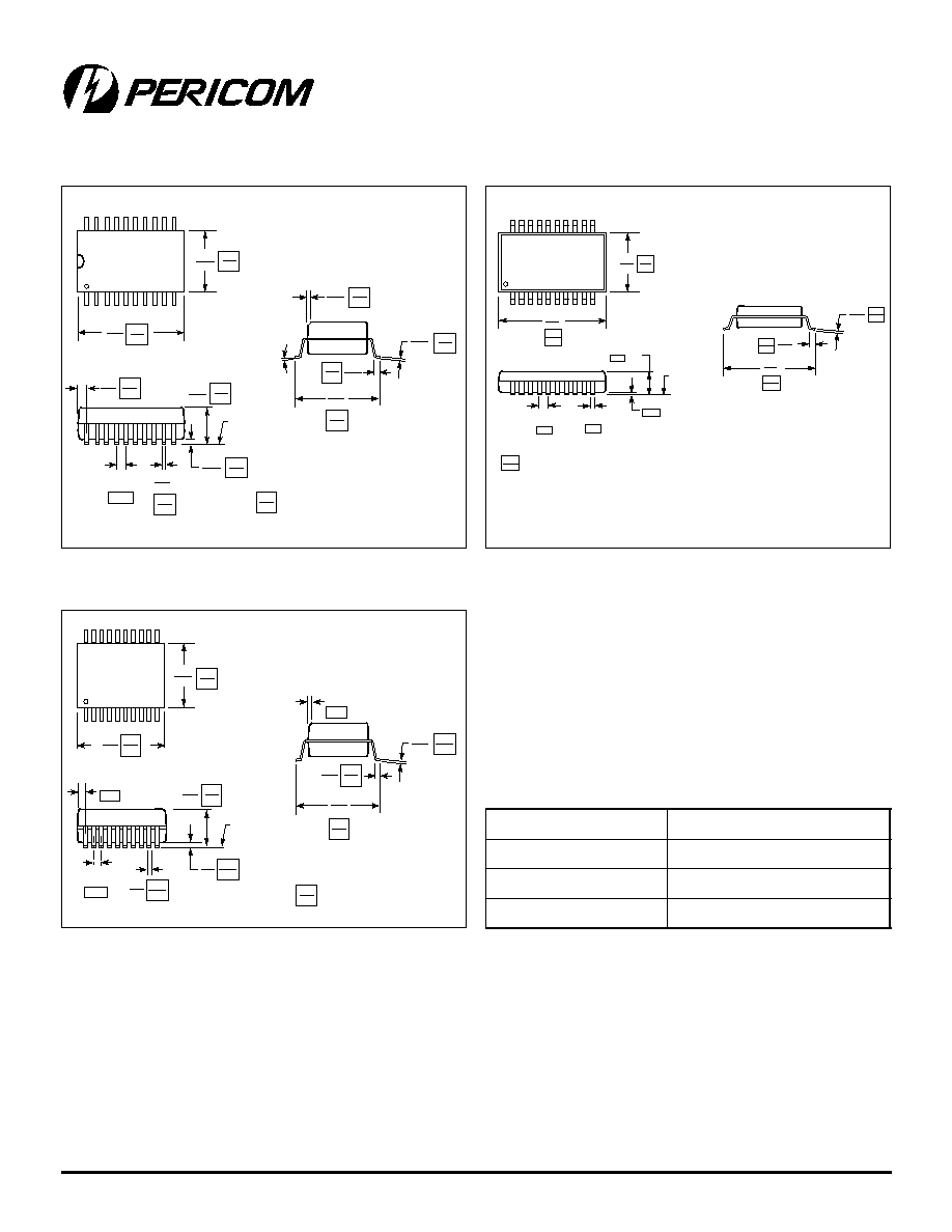
SEATING
PLANE
.050
BSC
1
20
0-8�
.2914
.2992
X.XX
X.XX
DENOTES CONTROLLING
DIMENSIONS IN MILLIMETERS
7.40
7.60
.496
.511
12.60
12.99
1.27
.0926
.1043
2.35
2.65
.394
.419
10.00
10.65
.0040
.0118
0.10
0.30
.013
.020
0.33
0.51
.010
.029
0.254
0.737
.0091
.0125
0.23
0.32
0.41
1.27
.016
.050
x 45�
.020
.030
0.508
0.762
REF
.337
.344
.053
.069
.004
.010
SEATING
PLANE
.025
BSC
.007
.010
.228
.244
.150
.157
1
20
.016
.050
X.XX
X.XX
DENOTES DIMENSIONS
IN MILLIMETERS
0.635
8.56
8.74
1.35
1.75
5.79
6.19
0.41
1.27
0.101
0.254
.008
.012
0.203
0.305
3.81
3.99
0.178
0.254
.058
1.47
.015 x 45�
0.38
REF
.272
.295
.078
.002
SEATING
PLANE
.0098
Max.
.0256
BSC
.022
.037
.004
.009
.291
.322
1
20
.197
.220
0.25
X.XX
X.XX
DENOTES DIMENSIONS
IN MILLIMETERS
0.050
7.40
8.20
0.55
0.95
0.09
0.25
5.00
5.60
2.00
6.90
7.50
0.65
Max
Min
20-Pin SOIC (S20) Package
20-Pin SSOP (H20) Package
20-Pin QSOP (Q20) Package
e
d
o
C
g
n
i
r
e
d
r
O
e
p
y
T
e
g
a
k
c
a
P
S
D
7
0
8
3
T
C
F
9
4
I
P
C
I
O
S
e
d
i
w
li
m
0
0
3
n
i
p
-
0
2
Q
D
7
0
8
3
T
C
F
9
4
I
P
P
O
S
Q
e
d
i
w
li
m
0
5
1
n
i
p
-
0
2
H
D
7
0
8
3
T
C
F
9
4
I
P
P
O
S
S
e
d
i
w
li
m
9
0
2
n
i
p
-
0
2
Ordering Information