 | –≠–ª–µ–∫—Ç—Ä–æ–Ω–Ω—ã–π –∫–æ–º–ø–æ–Ω–µ–Ω—Ç: PI5A100QE | –°–∫–∞—á–∞—Ç—å:  PDF PDF  ZIP ZIP |
1
PS7012H 08/30/04
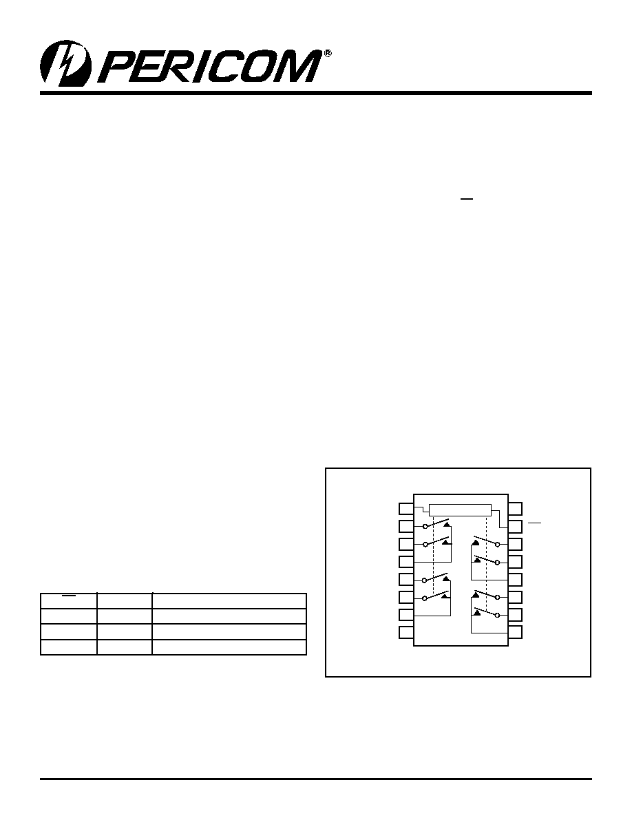
Block Diagram, Pin Configuration
Features
∑ Single Supply Operation (+2V to +6V)
∑ Rail-to-Rail Analog Signal Dynamic Range
∑ Low On-Resistance (6 typ with 5V supply) Minimizes
Distortion and Error Voltages
∑ On-Resistance Matching Between Channels, 0.4 Typ.
∑ On-Resistance Flatness, <2 Typ.
∑ Low Charge Injection Reduces Glitch Errors, Q = 6pC Typ.
∑ Replaces Mechanical Relays
∑ High Speed. t
ON
, 8ns Typ.
∑ Low Crosstalk: -100dB @ 10 MHz
∑ Low Off-Isolation: -57dB @ 10 MHz
∑ Wide -3dB Bandwidth: 230 MHz
∑ High-Current Channel Capability: >100mA
∑ TTL/CMOS Logic Compatible
∑ Low Power Consumption (0.5µW typ.)
∑ Packaging (Pb-free & Green Available):
-16-pin QSOP (Q)
-16-pin SOIC (W)
Applications
∑ Audio, Video Switching and Routing
∑ LAN Switches
∑ Telecommunication Systems
∑ Battery-Powered Systems
Truth Table
EN
IN
ON Switch
0
0
NC
1
, NC
2
, NC
3
, NC
4
0
1
NO
1
, NO
2
, NO
3
, NO
4
1
X
None. Disabled
Notes:
1. Switches shown for logic "0" input.
2. NC = Normally Closed; NO = Normally Open
PI5A100
Precision, Wide-Bandwidth
Quad SPDT Analog Switch
Description
The PI5A100 is an improved Quad Single-pole double-throw
(4SPDT) CMOS analog switch designed to operate with a single
+2V to +6V power supply. The EN pin may be used to place all
switches in a high-impedance state. This high precision device
is ideal for low-distortion audio, video, and data switching and
routing.
Each switch conducts current equally well in either direction
when on. In the off state each switch blocks voltages up to the
power-supply rails.
The PI5A100 is fully specified with +5V, and +3.3V supplies. With
+5V, it guarantees less than 10 On-Resistance. On-Resistance
matching between channels is within 2. On-Resistance flatness
is less than 4 over the specified range. The PI5A100 guarantees
fast switching speeds (t
ON
< 12ns).
The PI5A100 is available in the narrow-body SOIC and QSOP
packages for operation over the industrial (-40∞C to +85∞C) tem-
perature range.
1
2
3
4
5
6
7
8
16
15
14
13
12
11
10
9
V
CC
EN
NC
4
NO
4
COM
4
NC
3
NO
3
COM
3
IN
NC
1
NO
1
COM
1
NC
2
NO
2
COM
2
GND
Decoder
2
PS7012H 08/30/04
PI5A100
Precision, Wide-Bandwidth, Quad SPDT Analog Switch
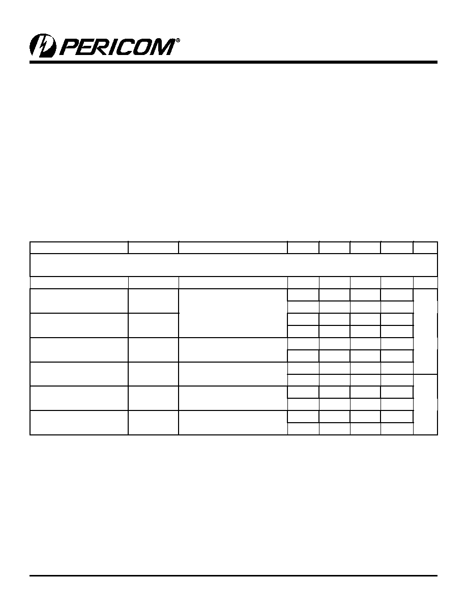
Absolute Maximum Ratings
Thermal Information
Continuous Power Dissipation
Narrow SOIC & QSOP
(derate 8.7mW/∫C above +70∫C) . . . . . . . . . . . . . . . . . 650mW
Storage Temperature . . . . . . . . . . . . . . . . . . . . -65
∫
C to +150
∫
C
Lead Temperature (soldering, 10s) . . . . . . . . . . . . . . . . +300
∫
C
Voltages Referenced to Gnd
V
CC
........................................................................-0.5V to +7V
V
IN
, V
COM
, V
NC
, V
NO
(1)
..............................-0.5V to V
CC
+2V
..................................................or 30mA, whichever occurs first
Current (any terminal except COM, NO, NC).................. 30mA
Current, COM, NO, NC
(pulsed at 1ms, 10% duty cycle)..................................... 120mA
Notes:
1. Signals on NC, NO, COM, or IN exceeding V
CC
or GND are clamped by internal diodes. Limit forward diode current to 30mA.
2. Caution: Stresses beyond those listed under "Absolute Maximum Ratings" may cause permanent damage to the device. This is a stress
only rating and operation of the device at these or any other conditions beyond those indicated in the operational sections of this speci fication
is not implied.
Electrical Specifications - Single +5V Supply
(V
CC
= +5V ±10%, GND = 0V, V
INH
= 2.4V, V
INL
= 0.8V)
Parameter
Symbol
TestConditions
Temp. Min.
(1)
Typ.
(2)
Max.
(1)
Units
Analog Switch
Analog Switch Range
(1)
V
ANALOG
Full
0
V
CC
V
On-Resistance
R
ON
V
CC
= 4.5V, I
COM
= -30mA,
V
NO
or V
NC
= +2.5V
25
8
10
Full
12
On-Resistance Match Be-
tween Channels
(6)
R
ON
25
0.8
2
Full
4
On-Resistance Flatness
(5)
R
FLAT(ON)
V
CC
= 5V, I
COM
= -30mA,
V
NO
or V
NC
= +2.5V
25
2
3
Full
4
NO or NC OFF Leakage
(6)
I
NO(OFF)
or
I
NC(OFF)
V
CC
= 5.5C, I
COM
= 0V,
V
NO
or V
NC
= 4.5V
25
0.07
Full
-80
80
nA
COM OFF Leakage
Current
(6)
I
COM(OFF)
V
CC
= 5.5V, I
COM
= 4.5V,
V
NO
or V
NC
= ± 4.5V
25
0.01
Full
-80
80
COM ON Leakage
Current
(6)
I
COM(ON)
V
CC
= 5.5V, I
COM
= 4.5V,
V
NO
or V
NC
= ± 4.5V
25
0.016
Full
-80
80
3
PS7012H 08/30/04
PI5A100
Precision, Wide-Bandwidth, Quad SPDT Analog Switch
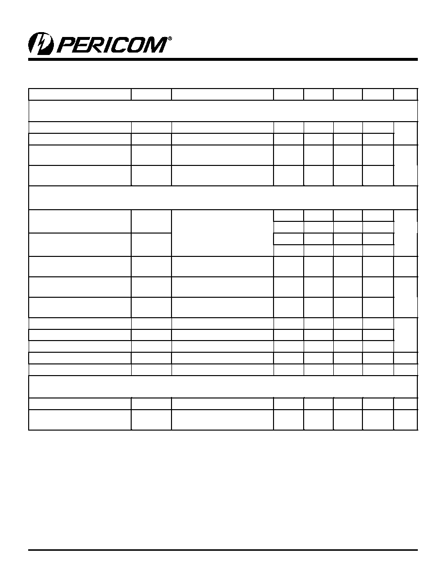
Electrical Specifications - Single +5V Supply
(V
CC
= +5V ±10%, GND = 0V, V
INH
= 2.4V, V
INL
= 0.8V) CONTINUED
Parameter
Symbol
TestConditions
Temp. Min.
(1)
Typ.
(2)
Max.
(1)
Units
Logic Input
Input High Voltage
V
IH
Guaranteed logic High Level
Full
2
V
Input Low Voltage
V
IL
Guaranteed logic Low Level
0.8
Input Current with Input Voltage
High
I
INH
V
IN
= 2.4V, all others = 0.8V
Full
-1
0.005
1
µA
Input Current with Input Voltage
Low
I
INL
V
IN
= 0.8V, all others = 2.4V
-1
0.005
1
Dynamic
Turn-On Time
t
ON
V
CC
= 5V, See Figure 1
25
8
15
ns
Full
20
Turn-Off Time
t
OFF
25
3.5
7
Full
10
Charge Injection
(3)
Q
C
L
= 1nF, V
GEN
= 0V,
R
GEN
= 0, See Figure 2
25
10
pC
Off Isolations
O
IRR
R
L
= 50, C
L
= 5pF,
f = 10MHz, See Figure 3
-57
dB
Crosstalk
(8)
X
TALK
R
L
= 50, C
L
= 5pF,
f = 10MHz, See Figure 4
-100
NC or NO Capacitance
C
(OFF)
f=1kHz, See Figure 5
8
pF
COM OFF Capacitance
C
COM(OFF)
14
COM ON Capacitance
C
COM(ON
) f = 1kHz, See Figure 6
18
-3db Bandwidth
BW
R
L
= 50 See Figure 7
Full
230
MHz
Distortion
D
R
L
= 10k
0.2
%
Supply
Power-Supply
V
CC
Full
2
6
V
Postitive Supply Current
I
CC
V
CC
= 5.5V, V
IN
= 0V or V
CC
,
all channels on or off
1
µA
Notes:
1. The algebraic convention, where the most negative value is a minimum and the most positive is a maximum, is used in this data sheet.
2. Typical values are for DESIGN AID ONLY, not guaranteed or subject to production testing.
3. Guaranteed by design
4. R
=
R
max - R
min
5. Flatness is defined as the difference between the maximum and minimum value of On-Resistance measured.
6. Leakage parameters are 100% tested at maximum rated hot temperature and guaranteed by correlation at +25∫C.
7. Off Isolation = 20log
10
[ V
COM
/ (V
NO
or V
NC
)
]. See figure 3.
8. Between any two switches. See figure 4.-
4
PS7012H 08/30/04
PI5A100
Precision, Wide-Bandwidth, Quad SPDT Analog Switch
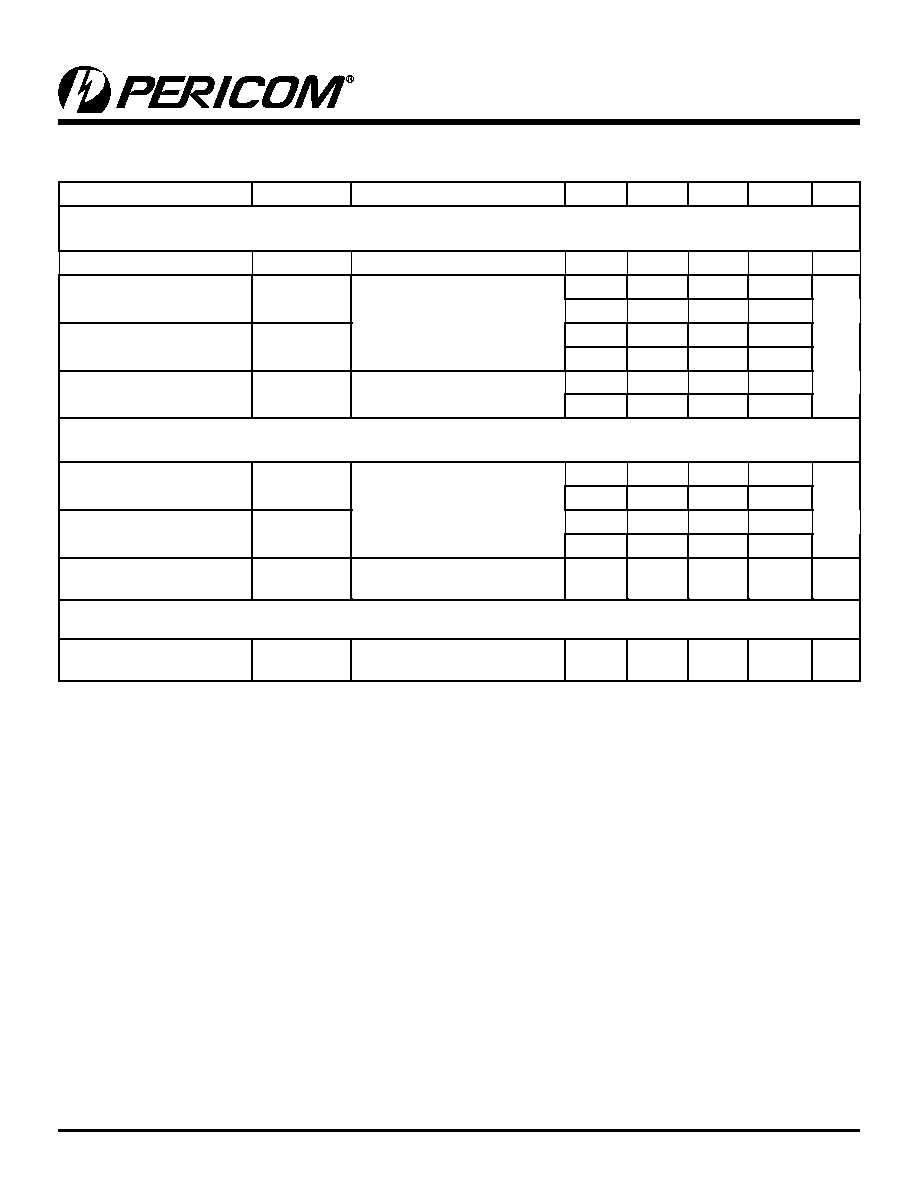
Electrical Specifications - Single +3.3V Supply
(V
CC
= +5V ±10%, GND = 0V, V
INH
= 2.4V, V
INL
= 0.8V)
Parameter
Symbol
TestConditions
Temp. Min.
(1)
Typ.
(2)
Max.
(1)
Units
Analog Switch
Analog Switch Range
(1)
0
V
CC
V
On-Resistance
R
ON
V
CC
= 4.5V, I
COM
= -30mA,
V
NO
or V
NC
= +2.5V
25
12
18
Full
On-Resistance Match Be-
tween Channels
(6)
R
ON
25
5
Full
On-Resistance Flatness
(5)
R
FLAT(ON)
V
CC
= 5V, I
COM
= -30mA,
V
NO
or V
NC
= +2.5V
25
2
4
Full
5
Dynamic
Turn-On Time
t
ON
V
CC
= 5V, See Figure 1
25
14
25
ns
Full
40
Turn-Off Time
t
OFF
25
4.5
12
Full
20
Charge Injection
(3)
Q
C
L
= 1nF, V
GEN
= 0V,
R
GEN
= 0, See Figure 2
25
5
10
pC
Supply
Postitive Supply Current
I
CC
V
CC
= 3.6V, V
IN
= 0V or V
CC
,
all channels on or off
Full
1
µA
5
PS7012H 08/30/04
PI5A100
Precision, Wide-Bandwidth, Quad SPDT Analog Switch
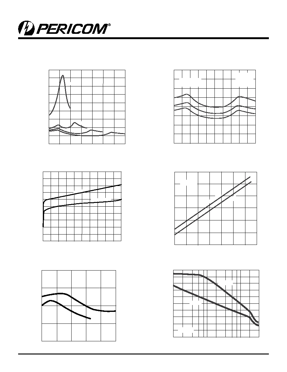
Typical Operating Characteristics
(T
A
=+25∫C, unless otherwise noted)
Charge Injection vs. Analog Voltage
Leakage Current vs. Temperature
Crosstalk and Off-Isolation vs. Frequency
R
ON
vs. V
COM
R
ON
vs. V
COM
and Temperature
Leakage Currents vs. Analog Voltage
20
V
10
30
40
+5V
+7V
COM
1
2
3
4
5
6
7
(V)
Vcc = +2V
+3.3V
R
ON
8
4
12
16
1
2
3
4
5
R
O
N
0
A
B
C
0
V
CC
= +5V
A: T
A
= 90∞C
B: T
A
= 25∞C
C: T
A
= -40∞C
-40
40
80
10nA
1nA
100pA
10pA
1pA
0.1pA
0.01pA
Temperature (∞C)
L
e
a
k
a
g
e
I
I
0
CO
M(
ON
)
CO
M(
OF
F)
CC
=
+5V
V
20
16
8
0
-8
-16
0
1
2
3
4
5
Temperature (∞C)
Leakage (pA)
IA(ON) or IB(ON)
IA(ON) or IB
(ON)
15
10
5
0
-5
0
1
2
3
4
5
Q-Charge Injection (pC)
V
CC
= 3.3V
V
CC
= 5V
V
COM
(V)
-100
-80
-60
-40
-20
0
1
2
4
6 8 10
20
40 60 80 100
200
Off Isolation
Crosstalk
VCC = 5V
Frequency (MHz)
(dB)
6
PS7012H 08/30/04
PI5A100
Precision, Wide-Bandwidth, Quad SPDT Analog Switch
R
ON
vs. V
COM
and Single Supply
Switching Times vs. Temperature
Insertion Loss vs. Frequency
Input Switching Threshold vs. Supply Voltage
Supply Current vs. Temperature
10
1
0.1
0.01
0.001
-40
0
40
80
Temperature (∞C)
V
CC
= +5V
I
CC
(nA)
0
-1
-2
-3
-4
-5
-6
-7
-8
-9
-10
3
1
6
10
30
60 100
300
I
n
s
e
r
t
i
o
n
L
o
s
s
(
d
B
)
Frequency (MHz)
R = 50!
-
3dB Point
L
V = +5V
CC
4
3
2
1
0
5
4
3
7
5
6
V
IN,
(V)
V
CC
(V)
4.5
7
5
5.5
6.5
6
4
3.5
20
15
10
5
0
25
3
t
ON,
t
OFF
(ns)
V
CC
(V)
t
ON,
t
OFF
-40
0
5
10
15
20
0
40
80
120
Temperature (∞C)
t
ON
t
OF
F
(ns)
t
ON
t
OFF
7
PS7012H 08/30/04
PI5A100
Precision, Wide-Bandwidth, Quad SPDT Analog Switch
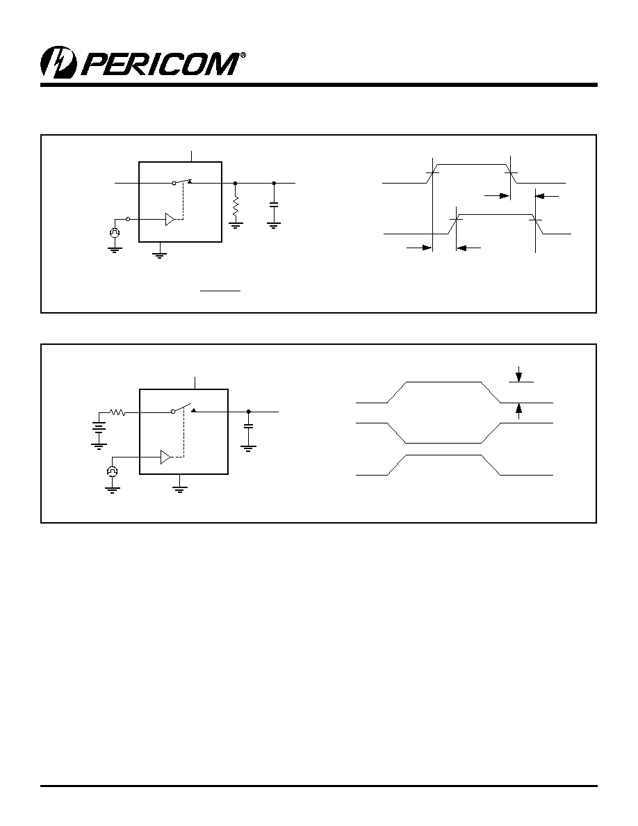
Test Circuits/Timing Diagrams
Figure 1. Switching Time
Figure 2. Charge Injection
Vcc
+5V
NO
GND
or NC
COM
+3V*
Logic
Input
IN
tr <20ns
tf <20ns
V
OUT
= V
NO
R
L
R
L +
R
ON
(
)
C
L
INCLUDES FIXTURE AND STRAY CAPACITANCE
V
OUT
R
L
100Ohm
C
L
15pF
LOGIC INPUT WAVEFORMS INVERTED FOR
SWITCHES THAT HAVE OPPOSITE LOGIC
* 1.5V FOR 3.3V SUPPLY
t
OFF
t
ON
V
OUT
90%
90%
Logic
Input
Switch
Output
+3V
0V
0V
50%
Switch
Input
V+
+5V
NO or
GND
NC
COM
V
OUT
C
L
1nF
V
OUT
V
OUT
IN
V
GEN
ON
ON
OFF
OFF
OFF
OFF
IN
Q = (V
OUT
)(C
L
)
IN
Logic
Input
.1µF
R
GEN
8
PS7012H 08/30/04
PI5A100
Precision, Wide-Bandwidth, Quad SPDT Analog Switch
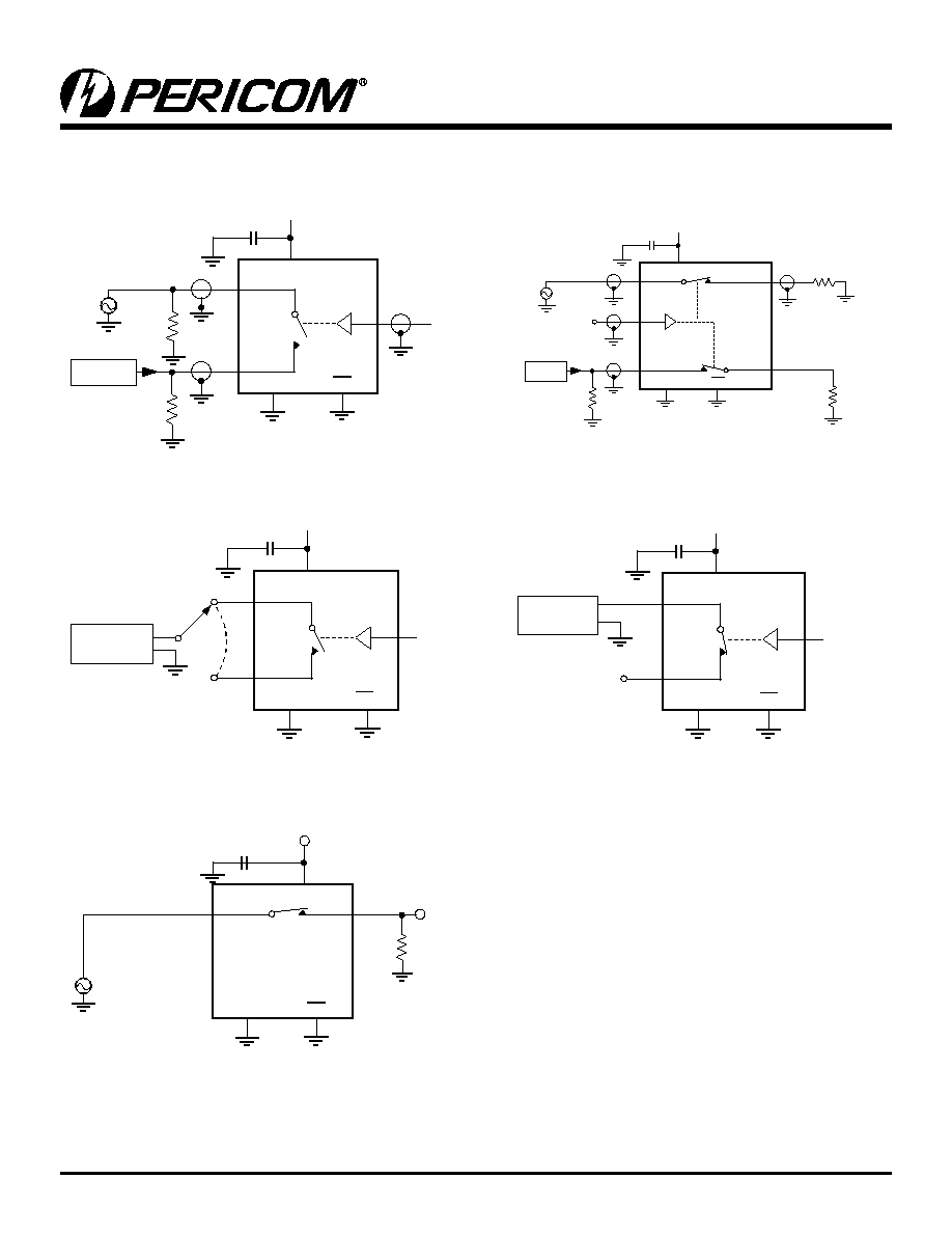
Test Circuits/Timing Diagrams (continued)
Figure 3. Off Isolation
Figure 5. Channel-Off Capacitance
Figure 4. Crosstalk
Figure 6. Channel-On Capacitance
Figure 7. Bandwidth
V+
+5V
Analyzer
GND
EN
N02
COM1
10nF
COM
Signal
Generator 0dBm
0V or
2.4V
COM2
IN
N01
NC
50
Ohm
10Ohm
50Ohm
V+
+5V
NC
Capacitance
Meter
GND
EN
or NO
COM
10nF
IN
0V or
2.4V
f = 1MHz
V+
+5V
NC
Capacitance
Meter
GND
EN
or NO
COM
10nF
IN
0V or
2.4V
f = 1kHz
V+
+5V
NC
Analyzer
GND
EN
or NO
COM
10nF
IN
COM
50Ohm
50Ohm
0V or
2.4V
V
CC
+5V
NC
GND
EN
or NO
10nF
Rg = 50Ohm
COM
R
L
10Ohm
Vo
9
PS7012H 08/30/04
PI5A100
Precision, Wide-Bandwidth, Quad SPDT Analog Switch
Applications Information
Overvoltage Protection
Proper power-supply sequencing is recommended for all CMOS
devices. Do not exceed the absolute maximum ratings, because
stresses beyond the listed ratings may cause permanent damage
to the devices. Always sequence V+ on first, followed by V-, and
then logic inputs. If power-supply sequencing is not possible, add
two small signal diodes or two current limiting resistors in series
with the supply pins for overvoltage protection (Figure 8). Adding
diodes reduces the analog signal range, but low switch resistance
and low leakage characteristics are unaffected.
RGB Switch
Figure 9 illustrates a simple low cost RGB switch. The RGB -
to-Composite Decoder produces either NTSC or S-VHS video
from an RGB source. Asingle PI5A100 selects one of the two
video sources to produce either SVHS, Composite or RGB video
outputs. The low insertion loss of the PI5A100 eliminates the need
for expensive input/output buffers.
Figure 8: Overvoltage protection is accomplished using two ex-
ternal blocking diodes or two current limiting resistors.
Figure 9: The single PI5A100 is used to select SVHS, VGA or Composite video outputs.
V+
Positive Supply
COM
NO
Vg
V-
Select
C
Composite
Connector
S-Video
Connector
Composite
RGB to
Composite
Encoder
SVGA
R-G-B
Sync
R
B
+5V
G
Sync
4
Y
PI5A100
H-Sync-0.3V
G or Composite 0.714V
R or Luma 0.7V
B or Chroma 0.28V
VGA
Connect or
10
PS7012H 08/30/04
PI5A100
Precision, Wide-Bandwidth, Quad SPDT Analog Switch
Applications
Audio Muting Function
Figure 8 shows the PI5A100 in an audio card muting application.
The original problem was one of excessive popping/clicking noise
appearing when connecting disconnecting external loads, and at
power on/off. The PI5A100 performs a muting function by grounding
the outputs at power on/off and during the transition time. The
32 headset impedance demands a very low and very flat switch-
on resistance to reduce THD and signal loss.
Figure 10: The PI5A100 momentarily mutes the stereo outputs by connecting them to ground during transition times.
Paralleling two sections of the PI5A100 produces a Ron of 2.5
with an unsurpassed
±0.5 flatness.
To handle AC signals it was necessary to power the device with
±3V provided by two Zener diodes: Z1 and Z2. The select and
Enable control signals are shifted by using twpo 2.5V Zener diodes
Z3,Z4 and pull down resistors connected to -3V.
Vcc
GND
Select
J2
J1
Z1/Z2 - Dual SMT 3.0V Zener
32!
22k!
2.5V
-3V
Stereo Audio
Output
2.5V
Z3
Z4
Enable
Z1
Z2
+5V
-5V
-3V
Stereo Audio
Input
From DAC
10k
11
PS7012H 08/30/04
PI5A100
Precision, Wide-Bandwidth, Quad SPDT Analog Switch
.189
.197
.053
.069
.004
.010
SEATING
PLANE
.025
BSC
.007
.010
.228
.244
1
16
.150
.157
.016
.050
X.XX
X.XX
DENOTES DIMENSIONS IN MILLIMETERS
0.635
4.80
5.00
1.35
1.75
5.79
6.19
0.101
0.254
.008
.012
0.203
0.305
3.81
3.99
0.178
0.254
0.38
0.41
1.27
.008
0.203
.015 x 45
∞
REF
Detail A
Detail A
.008
0.20
MIN.
Guage Plane
.010
0.254
.041
1.04
REF
.016
.035
0.41
0.89
0∞-6∞
.008
.013
0.20
0.33
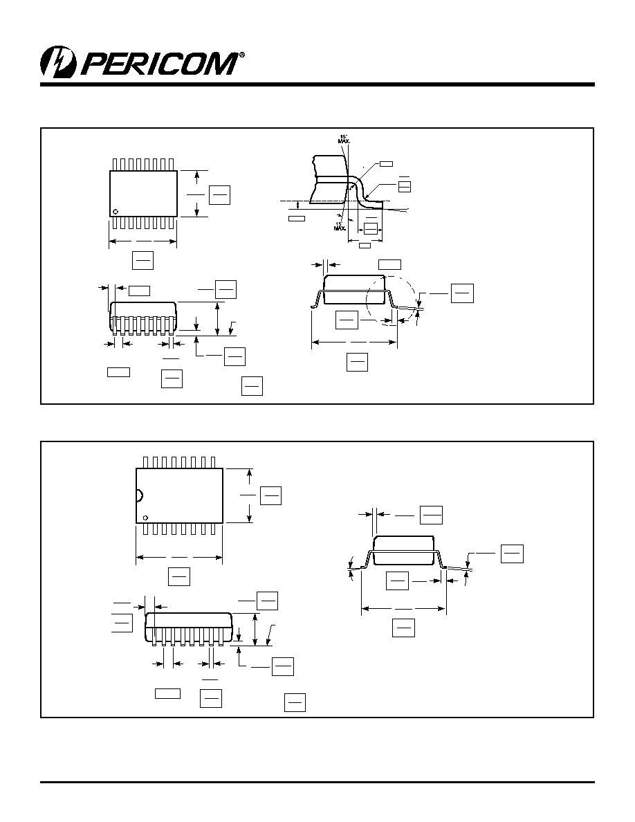
Packaging Mechanical: 16-Pin QSOP (Q)
Packaging Mechanical: 16-Pin SOIC (W)
SEATING PLANE
.050
BSC
1
16
0-8∞
.149
.157
X.XX
X.XX
DENOTES DIMENSIONS
IN MILLIMETERS
3.78
3.99
.386
.393
9.80
10.00
1.27
.053
.068
1.35
1.75
.2284
.2440
5.80
6.20
.0040
.0098
0.10
0.25
.013
.020
.0155
.0260
0.330
0.508
0.393
0.660
.0075
.0098
0.25
0.50
.0099
.0196
x 45∞
0.19
0.25
.016
.050
0.41
1.27
REF
12
PS7012H 08/30/04
PI5A100
Precision, Wide-Bandwidth, Quad SPDT Analog Switch
Ordering Information
Ordering Code
Package Code
Package Description
PI5A100W
W
16-pin SOIC
PI5A100Q
Q
16-pin QSOP
PI5A100QE
Q
Pb-free & Green, 16-pin QSOP
Notes:
1. Thermal characteristics can be found on the company web site at www.pericom.com/packaging/
2,. Number of Transistors = TBD
Pericom Semiconductor Corporation ∑ 1-800-435-2336 ∑ www.pericom.com