 | –≠–ª–µ–∫—Ç—Ä–æ–Ω–Ω—ã–π –∫–æ–º–ø–æ–Ω–µ–Ω—Ç: PI5A101Q | –°–∫–∞—á–∞—Ç—å:  PDF PDF  ZIP ZIP |
1
PS7079F 09/22/04
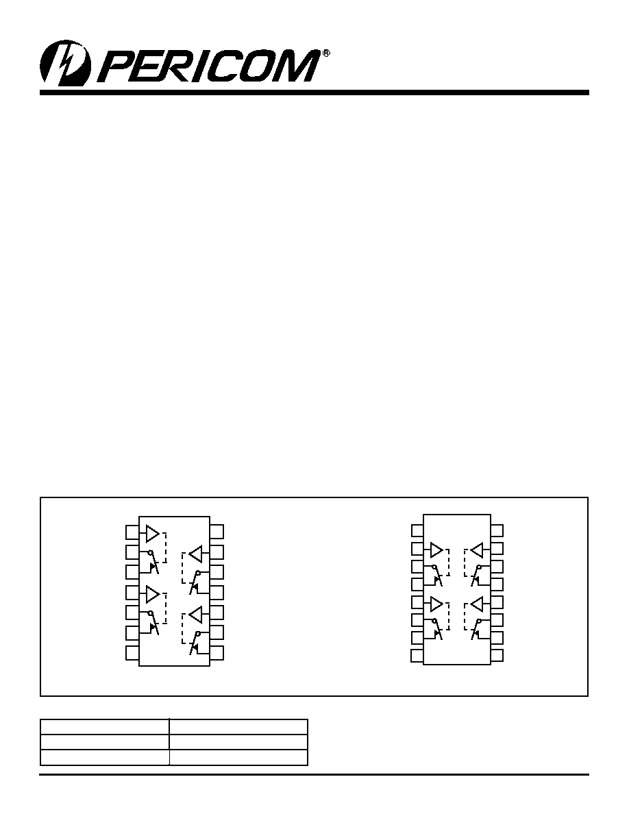
Pin Configurations
Features
∑ Rail-To-Rail operation
∑ Pin-compatible with 3125 Bus Switch & 74 series 125
∑ Single-Supply operation: 2V to 6V
∑ Low On-Resistance: 8 typical @ 5V
∑ Tight match between channels: 0.9 typical
∑ R
ON
flatness: 3 typical
∑ Low power consumption: 0.5µ-ohm typical
∑ High Speed, T
ON
= 8ns typical
∑ High-current channel capability: >100mA
∑ Wide bandwidth: >200 MHz
∑ Packaging (Pb-free & Green available):
-14-pin SOIC (W)
-16-pin QSOP (Q)
Applications
∑ Instrumentation, ATE
∑ Audio Switching and Routing
∑ Telecommunications Systems
∑ Data Communications
∑ Battery-Powered Systems
∑ Replaces Mechanical Relays
Description
Pericom Semiconducto's PI5A101 is an all-purpose analog switch
designed for single-supply operation from +2V to +6V. This switch
is ideal for audio, video, and data switching and routing.
The PI5A101 is a quad SPST (single-pole, single-throw)
NC (normally closed) function.
When on, each switch conducts current equally well in either
direction. When off, they block voltages up to the power-
supply rails.
The PI5A101 is fully specified with +5V and +3.3V supplies.
With +5V the R
ON
is 8 typical, making it ideal for replacing
mechanical relays in data communications, test equipment, and
instrumentation applications. Matching between channels is
better than 2. R
ON
flatness is better than 4 over the specified
range.
These analog switches also offer wide bandwidth (>200 MHz high
speed (T
ON
>15ns), and low charge injection (Q >10pC).
The PI5A101 is available in the narrow-body 14-pin small SOIC
and 16-pin QSOP packages for operation over the industrial
(≠40∞C to +85∞C) temperature range.
Switches show for logic "0" input
NIC = Not Internally Connected
Precision Wide-Bandwidth Analog Switch
PI5A101
1
2
3
4
5
7
6
IN
1
COM
1
NC
1
IN
2
OM
2
NC
2
GND
12
13
14
11
10
9
8
V
CC
COM
NC
4
IN
3
COM
NC
3
IN
4
16 V
CC
COM
NC
4
IN
3
COM
NC
3
IN
4
9 NIC
12
13
14
11
10
15
1
2
3
4
5
7
6
8
SOIC
Top View
QSOP
IN
1
COM
1
NC
1
IN
2
OM
2
NC
2
GND
NIC
Truth Table
Logic
Switch
0
ON
1
OFF
2
PS7079F 09/22/04
PI5A101
Precision Wide-bandwidth
Analog Switch
Electrical Specifications - Single +5V Supply
(V
CC
= +5V ± 10%, GND = 0V, V
INH
= 2.4V, V
INL
= 0.8V)
Parameter
Symbol
Conditions
Temp.(∞C) Min.
(1)
Typ.
(2)
Max.
(1)
Units
Analog Switch
Analog Signal
Range
(3)
V
ANALOG
Full
0
V
CC
V
On-Resistance
R
ON
V
CC
= 4.5V,
I
COM
= -30mA,
V
NO
or V
NC
= +2.5V
25
8
10
Full
18
On-Resistance
Match Between
Channels
(4)
R
ON
25
0.9
2
Full
4
On-Resistance
Flatness
(5)
R
FLAT(ON)
V
CC
= 5V,
I
COM
= -30mA,
V
NO
or V
NC
= 1V, 2.5V, 4V
25
3
4
Full
5
NO or NC Off Leak-
age Current
(6)
I
NO(OFF)
or
I
NC(OFF)
V
CC
= 5.5V,
V
COM
= 0V,
V
NO
or V
NC
= 4.5V
25
0.05
nA
Full
-80
80
COM Off Leakage
Current
(6)
I
COM(OFF)
V
CC
= 5.5V,
V
COM
= + 4.5V,
V
NO
or V
NC
= ± 0V
25
0.05
Full
-80
80
COM On Leakage
Current
(6)
I
COM(ON)
V
CC
= 5.5V,
V
COM
= +4.5V
V
NO
or V
NC
= +4.5V
25
0.07
Full
-80
80
Logic Input
Input High Voltage
V
IH
Guaranteed logic High Level
Full
2
V
Input Low Voltage
V
IL
Guaranteed logic Low Level
Input Current with
Voltage High
I
INH
V
IN
= 2.4V, all others = 0.8V
0.8
µA
Input Current with
Voltage Low
I
INL
V
IN
= 0.8V, all others = 2.4V
-1
0.005
1
3
PS7079F 09/22/04
PI5A101
Precision Wide-bandwidth
Analog Switch
Electrical Specifications - Single +5V Supply
(V
CC
= +5V ± 10%, GND = 0V, V
INH
= 2.4V, V
INL
= 0.8V) (continued)
Parameter
Symbol
Conditions
Temp.(∫C) Min.
(1)
Typ.
(2)
Max.
(1)
Units
Dynamic
Turn-On Time
t
ON
V
CC
= 5V, see figure 1
25
8
15
ns
Full
20
Turn-Off Time
t
OFF
25
3.5
7
Full
10
Charge Injection
(3)
Q
C
L
= 1nF, V
GEN
= 0V,
R
GEN
= 0V, Figure 2
25
7
10
pC
Off Isolation
O
IRR
R
L
= 50, C
L
= 5pF, f = 10MHz,
see figure 3
-55
dB
Crosstalk
(8)
I
COM(OFF)
R
L
= 50, C
L
= 5pF, f = 10MHz,
see figure 4
-92
NC or NO Capacitance
C
(OFF)
f = 1kHz, see figure 5
8
pF
COM Off Capacitance
C
COM(OFF)
8
COM On Capacitance
C
COM(ON)
f = 1kHz, see figure 6
14
3-dB Bandwidth
BW
R
L
= 10k
Full
230
MHz
Distortion
(9)
D
0.03
%
Supply
Power-Supple Range
V
CC
Full
2
6
V
Positve Supply Current
I
CC
V
CC
= 3.6V, V
IN
= 0V or V+,
All Channels on or off
1
µA
4
PS7079F 09/22/04
PI5A101
Precision Wide-bandwidth
Analog Switch
Continuous Power Dissipation
Narrow SO & QSOP (derate 8.7mW/
∫
C above +70
∫
C) ...........650mW
Storage Temperature ................................................. -65
∫
C to +150
∫
C
Lead Temperature (soldering, 10s) .......................................... +300
∫
C
Voltages Referenced to GND
V
CC
.................................................................................≠0.5V to +7V
V
IN
, V
COM
, V
NC
(1)
................................................ ≠0.5V to V
CC
+2V
...........................................................or 30mA, whichever occurs first
Current (any terminal except COM, NO, NC)............................30mA
Current: COM, NO, NC (pulsed at 1ms, 10% duty cycle) .......120mA
Notes
1. Signals on NC, COM, or IN exceeding V
CC
or GND are clamped by internal diodes. Limit forward diode current to 30mA.
2. Caution: Stresses beyond those listed under "Absolute Maximum Ratings" may cause permanent damage to the device. This is a stress only
rating and operation of the device at these or any other conditions beyond those indicated in the operational sections of this specification is not
implied.
Absolute Maximum Ratings
Notes:
1. The algebraic convention, where most negative value is a minimum and most positive is a maximum, is used in this data sheet.
2. Typical values are for DESIGN AID ONLY, not guaranteed or subject to production testing.
3. Guaranteed by design
4. R
=
R
MAX - R
5. Flatness is defined as the difference between the maximum and minimum value of On-Resistance measured.
6. Leakage parameters are 100% tested at maximum rated hot temperature and guaranteed by correlation at +25∫C.
7. Off Isolation = 20log
10
V
B
/ V
A
. See Figure 3.
8. Between any two switches. See Figure 4.
9. D = R
FLAT(ON)
/R
L
.
Thermal Information
Electrical Specifications-Single +3.3V Supply
(V
CC
= +3.3V ± 10%, GND = 0V, V
INH
= 2.4V, V
INL
= 0.8V)
Parameter
Symbol
Conditions
Temp.(∞C) Min.
(1)
Typ.
(2)
Max.
(1)
Units
Analog Switch
Analog Signal Range
(3)
V
ANALOG
Full
0
V
CC
V
On-Resistance
R
ON
V
CC
= 3V,
I
COM
= -30mA,
V
NO
or V
NC
= 1.5V
25
7.2
18
Full
28
On-Resistance Match Be-
tween Channels
(4)
R
ON
25
0.2
2
Full
4
On-Resistance Flatness
(3,5)
R
FLAT(ON)
V
CC
= 3.3V,
I
COM
= -30mA,
V
NO
or V
NC
= 0.8V, 2.5V
25
2.72
10
Full
12
Dynamic
Turn-On Time
t
ON
V
CC
= 3.3V,
V
NO
or V
NC
= 1.5V,
see figure 1
25
7
25
ns
Full
40
Turn-Off Time
t
OFF
25
1
12
Full
20
Charge Injection
(3)
Q
C
L
= 1nF, V
GEN
= 0V,
R
GEN
= 0, Figure 2
25
1.6
10
pC
Supply
Positve Supply Current
I
CC
V
CC
= 3.6V, V
IN
= 0V or V
CC,
All Channels on or off
Full
1
µA
5
PS7079F 09/22/04
PI5A101
Precision Wide-bandwidth
Analog Switch
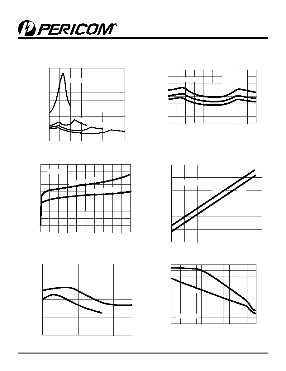
Typical Operating Characteristics
(TA = +25∫C, unless otherwise noted)
Charge Injection vs. Analog Voltage
Leakage Current vs. Temperature
Crosstalk and Off-Isolation vs. Frequency
R
ON
vs. V
COM
R
ON
vs. V
COM
and Temperature
Leakage Currents vs. Analog Voltage
8
4
12
16
1
2
3
4
5
R
O
N
(
o
h
m
)
V
COM
(V)
0
A
B
C
0
A: T
A
= 90∞C
B: T
A
= 25∞C
C: T
A
= ≠49∞C
V
CC
= +5V
20
10
30
40
+5V
+7V
1
2
3
4
5
6
7
V
CC
= +2V
+3.3V
R
ON
(ohm)
V
A
(V)
0
8
16
20
-8
-16
0
1
2
3
4
5
Leakage (pA)
N
O,
N
C,
VC
OM
(V)
V
CC
= +5V
I
A
(ON) or I
B
(ON)
I
A
(OFF) or I
B
(OFF)
-40
40
80
10nA
1nA
100pA
10pA
1pA
0.1pA
0.01pA
Temperature ∞C
Leakage
0
V
CC
= +5V
I
A
(OFF) or I
B
(OFF)
I
A
(ON) or I
B
(ON)
15
10
5
0
-5
0
1
2
3
4
5
Q-Charge Injection (pC)
V
CC
= 3.3V
V
CC
= 5V
V
COM
(V)
-100
-80
-60
-40
-20
0
2
1
4
10
6 8
20
40 60 80100 200
(dB)
Frequency (MHz)
V
CC
= +5V
Crosstalk
Off Isolation
6
PS7079F 09/22/04
PI5A101
Precision Wide-bandwidth
Analog Switch
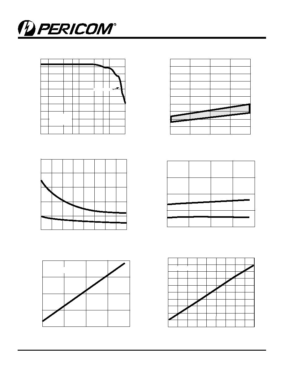
Switching Times vs. V
CC
Switching Times vs. Temperature
Insertion Loss vs. Frequency
Input Switching Threshold vs. Supply Voltage
Supply Current vs. Input Switching Frequency
Supply Current vs. Temperature
0
-1
-2
-3
-4
-5
-6
-7
-8
-9
-10
3
1
6 10
30
60 100
300
Insertion Loss (dB)
Frequency (MHz)
-3dB Point
V
CC
= +5V
R
L
= 50ohm
4.5
7
5
5.5
6.5
6
4
3.5
20
15
10
5
0
25
3
t
ON
t
OFF
VCC (V)
t
ON
, t
OFF
, (ns)
4
3
2
1
0
5
4
3
7
5
6
V
CC
(V)
V
OE
(V)
20
15
10
5
0
-40
0
40
80
Temperature (∫C)
t
ON
, t
OFF
, (ns)
10
1
0.1
0.01
0.001
-40
0
40
80
Temperature (∞C)
V
CC
= +5V
I
CC
(nA)
2.0
1.8
1.6
1.4
1.2
1.0
0.8
0.6
0.4
0.2
0.0
2
1
3
4
5
6
7
8
9
10
Frequency (MHz)
V
CC
= +5V
I
CC
(mA
)
7
PS7079F 09/22/04
PI5A101
Precision Wide-bandwidth
Analog Switch
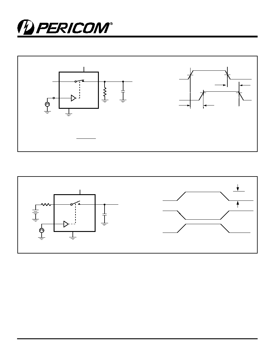
Test Circuits/Timing Diagrams
Figure 1. Switching Time
Figure 2. Charge Injection
V+
+5V
NC
GND
COM
R
GEN
V
OUT
C
L
1nF
V
OUT
V
OUT
IN
V
GEN
ON
ON
OFF
OFF
IN
OFF
OFF
Q = (V
OUT
)(C
L
)
IN
Logic
Input
V
CC
+5V
NC
GND
COM
+3V*
Logic
Input
IN
tr <20ns
tf <20ns
V
OUT =
V
NO
R
L
R
L +
R
ON
(
)
C
L
INCLUDES FIXTURE AND STRAY CAPACITANCE
V
OUT
RL
100-ohm
C
L
15pF
Logic Input Waveforms Inverted for
Switches that have Opposite Logic.
* 1.5V for 3.3V Supply
t
OFF
t
ON
V
OUT
90%
90%
Logic
Input
Switch
Output
+3V
0V
0V
50%
Switch
Input
8
PS7079F 09/22/04
PI5A101
Precision Wide-bandwidth
Analog Switch
Test Circuits/Timing Diagrams
(continued)
Figure 3. Off Isolation
Figure 5. Channel-Off Capacitance
Figure 6. Channel-On Capacitance
Figure 7. Bandwidth
Figure 4. Crosstalk
V+
+5V
Analyzer
GND
NC
COM
10nF
IN
50-ohm
0V or
2.4V
COM
50-ohm
V+
+5V
Capacitance
Meter
GND
NC
COM
10nF
IN
0V or
2.4V
f = 1kHz
V+
+5V
Capacitance
Meter
GND
NC
COM
10nF
IN
0V or
2.4V
f = 1kHz
V
CC
GND
NC
10nF
COM
+5V
V
O
RG = 50-ohm
R
L
= 50-ohm
V+
+5V
GND
NC
COM1
10nF
NO1
NO2
Signal Generator 0dBm
9
PS7079F 09/22/04
PI5A101
Precision Wide-bandwidth
Analog Switch
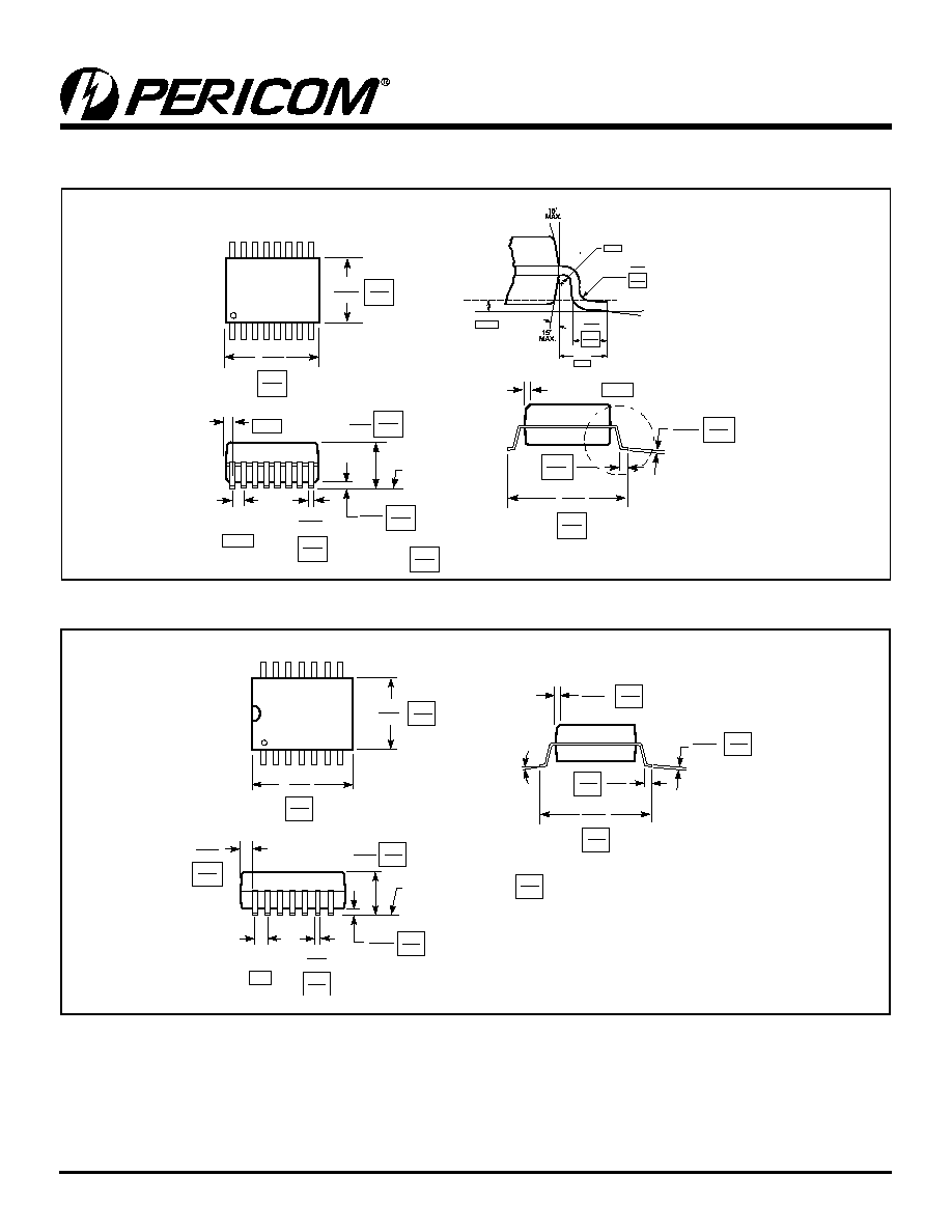
Packaging Mechanical: 16-Pin, QSOP (Q)
.189
.197
.053
.069
.004
.010
SEATING
PLANE
.025
BSC
.007
.010
.228
.244
1
16
.150
.157
.016
.050
X.XX
X.XX
DENOTES DIMENSIONS IN MILLIMETERS
0.635
4.80
5.00
1.35
1.75
5.79
6.19
0.101
0.254
.008
.012
0.203
0.305
3.81
3.99
0.178
0.254
0.38
0.41
1.27
.008
0.203
.015 x 45
∞
REF
Detail A
Detail A
.008
0.20
MIN.
Guage Plane
.010
0.254
.041
1.04
REF
.016
.035
0.41
0.89
0∞-6∞
.008
.013
0.20
0.33
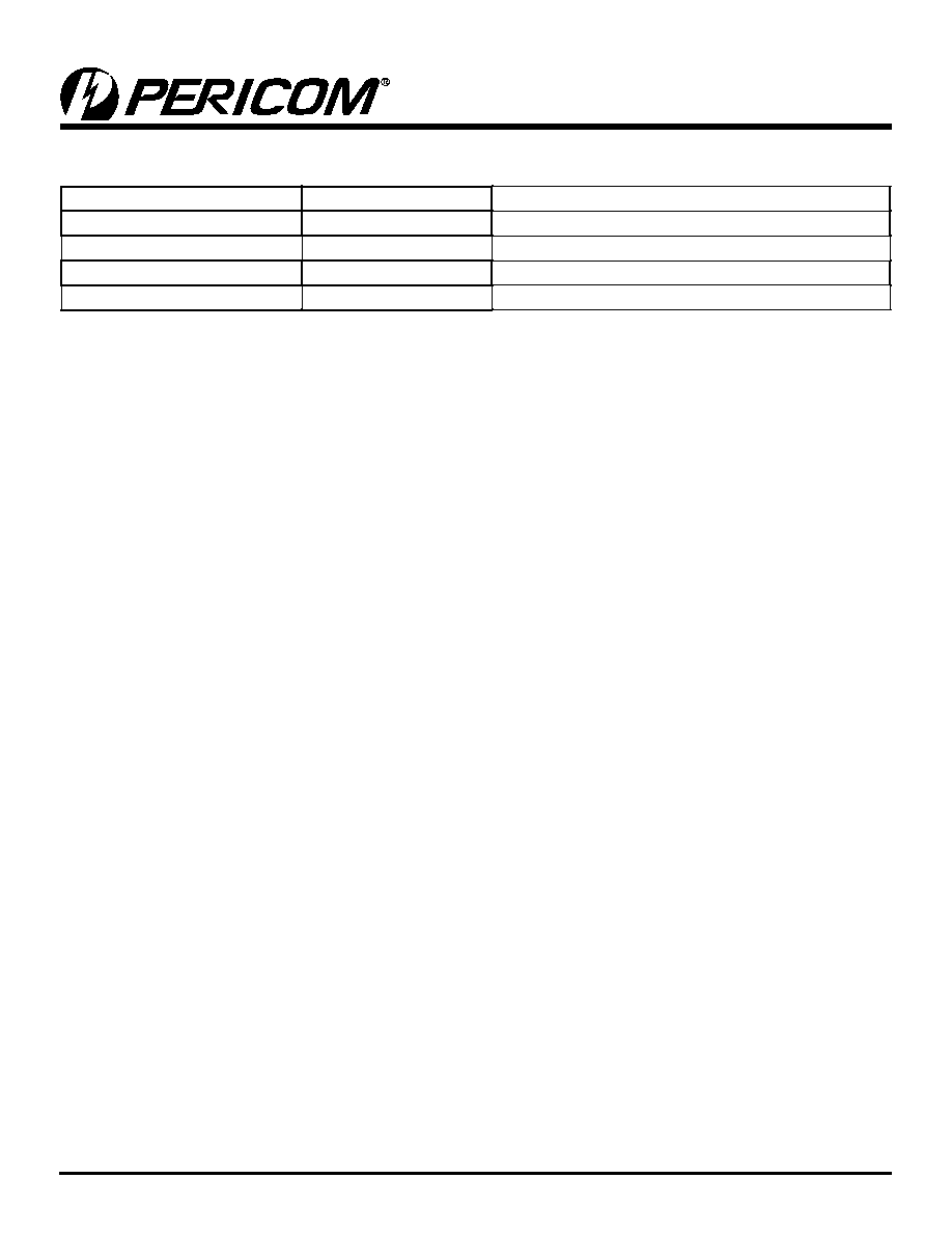
Packaging Mechanical: 14-Pin, SOIC (W)
SEATING PLANE
.050
BSC
1
14
x 45∞
0-8∞
.149
.157
X.XX
X.XX
DENOTES DIMENSIONS
IN MILLIMETERS
3.78
3.99
.336
.344
8.55
8.75
.0155
.026
0.393
0.660
1.27
.053
.068
1.35
1.75
.2284
.2440
5.80
6.20
.013
.020
0.330
0.508
.0040
.0098
0.10
0.25
.0099
.0196
0.25
0.50
.0075
.0098
0.19
0.25
.016
.050
0.41
1.27
REF
10
PS7079F 09/22/04
PI5A101
Precision Wide-bandwidth
Analog Switch
Ordering Information
Ordeing Code
Package Code
Package Description
PI5A101Q
Q
16-pin, QSOP
PI5A101QE
Q
Pb-free & Green, 16-pin, QSOP
PI5A101W
W
14-pin SOIC
PI5A101WE
W
Pb-free & Green, 14-pin SOIC
Pericom Semiconductor Corporation ∑ 1-800-435-2336 ∑ www.pericom.com
Notes:
1. Thermal characteristics can be found on the company web site at www.pericom.com/packaging/