 | –≠–ª–µ–∫—Ç—Ä–æ–Ω–Ω—ã–π –∫–æ–º–ø–æ–Ω–µ–Ω—Ç: PI5A124TX | –°–∫–∞—á–∞—Ç—å:  PDF PDF  ZIP ZIP |
1
PS8203G 10/19/04
Description
The PI5A121/PI5A122/PI5A124 are analog switches designed
for single-supply operation. These high-precision devices are
ideal for low-distortion audio, video, signal switching and rout-
ing.
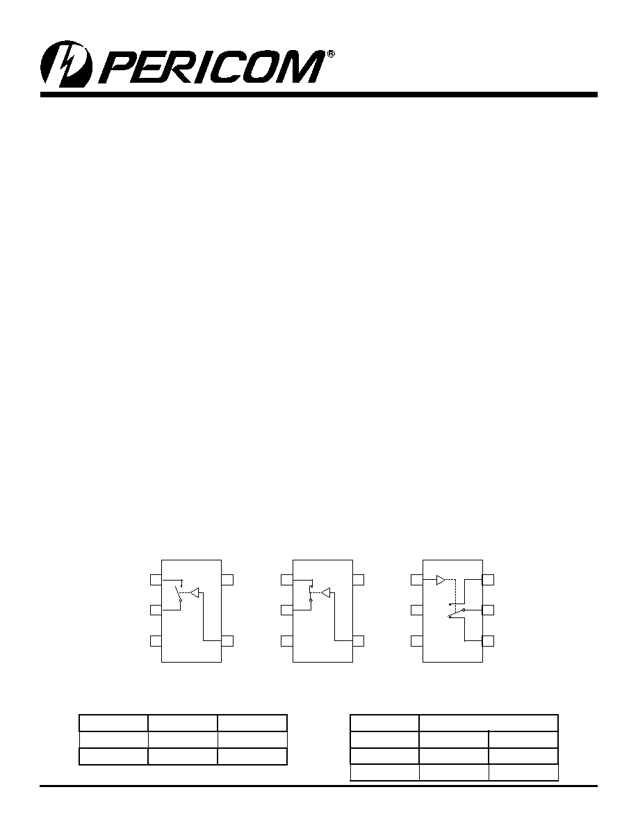
The PI5A121 is a single-pole throw (SPST) normally open (NO)
switch. The switch is open when IN is LOW. The PI5A122 is
a single-pole single-throw (SPST) normally closed (NC)
switch.
Each switch conducts current equally well in either direction
when on. When off, they block voltages up to V+.
These switches are fully specified with +5V, and +3.3V supplies.
With +5V, they guarantee <10 On-Resistance. On-Resistance
matching between channels is within 2. On-Resistance flatness
is less than 55 over the specified range. These switches also
guarantee fast switching speeds (t
ON
<20ns).
These products are available in 5-pin SC70 and/or 6-pin SOT23
plastic packages for operation over the industrial (-40
o
C to +85
o
C)
temperature range.
PI5A121/PI5A122/PI5A124
Wide Bandwidth Analog Switches
Features
∑ Single-Supply Operation (+2V to +6V)
∑ Rail-to-Rail Analog Signal Dynamic Range
∑ Low On-Resistance (6 typ. with 5V supply)
Minimizes Distortion and Error Voltages
∑ On-Resistance Flatness, 3 typ.
∑ Low Charge Injection Reduces Glitch Errors. Q = 4pC typ.
∑ High Speed. t
ON
= 10ns typ.
∑ Wide -3dB Bandwidth: 326 MHz (typ.)
∑ High-Current Channel Capability: >100mA
∑ TTL/CMOS Logic Compatible
∑ Low Power Consumption (0.5µW typ)
∑ Small outline transistor package minimizes board area
∑ Packaging (Pb-free & Green available):
- 5-pin 65-mil wide SOT23 (T) for PI5A121 and PI5A122
- 6-pin 65-mil wide SOT23 (T) for PI5A124
- 5-pin 50-mil wide SC70 (C) for PI5A121/PI5A122
Applications
∑ Audio, Video Switching, and Routing
∑ Battery-Powered Communication Systems
∑ Computer Peripherals
∑ Telecommunications
∑ Portable Instrumentation
∑ Mechanical Relay Replacement
∑ Cell Phones
∑ PDAs
Functional Diagrams, Pin Configurations and Truth Tables
Switches shown for Logic "0" input
COM
PI5A121
PI5A122
PI5A124
2
3
1
NO
GND
IN
V+
5
4
COM
IN
2
3
1
NC
GND
IN
V+
5
4
2
3
1
V+
GND
SOT23-6
NC
NO
COM
5
6
4
SOT23-5
SC70-5
SOT23-5
SC70-5
IN
PI5A121
PI5A122
0
OFF
ON
1
ON
OFF
PI5A124
LOGIC
NC
NO
0
ON
OFF
1
OFF
ON
2
PS8203G 10/19/04
PI5A121/PI5A122/PI5A124
Wide Bandwidth Analog Switch
Caution: Stresses beyond those listed under "Absolute Maximum Ratings" may cause permanent damage to the device. This is a stress only rating
and operation of the device at these or any other conditions beyond those indicated in the operational sections of this specification is not implied.
Absolute Maximum Ratings
Voltages Referenced to Gnd
V+ ..........................................................................-0.5V to +7V
V
IN
, V
COM
, V
NC
, V
NO
(Note 1)...................-0.5V to V
CC
+2V
or 30mA, whichever occurs first
Current (any terminal)..................................................... ±25mA
Peak Current, COM, NO, NC
(Pulsed at 1ms, 10% duty cycle)..................................... ±25mA
Note 1:
Signals on NC, NO, COM, or IN exceeding V+ or GND are clamped by
internal diodes. Limit forward diode current to 30mA.
Thermal Information
Continuous Power Dissipation
SOT23-6 (derate 7mW/∫C above +70∫C)........................ 550mW
Storage Temperature .........................................-65∫C to +150∫C
Lead Temperature (soldering, 10s) ................................. +300∫C
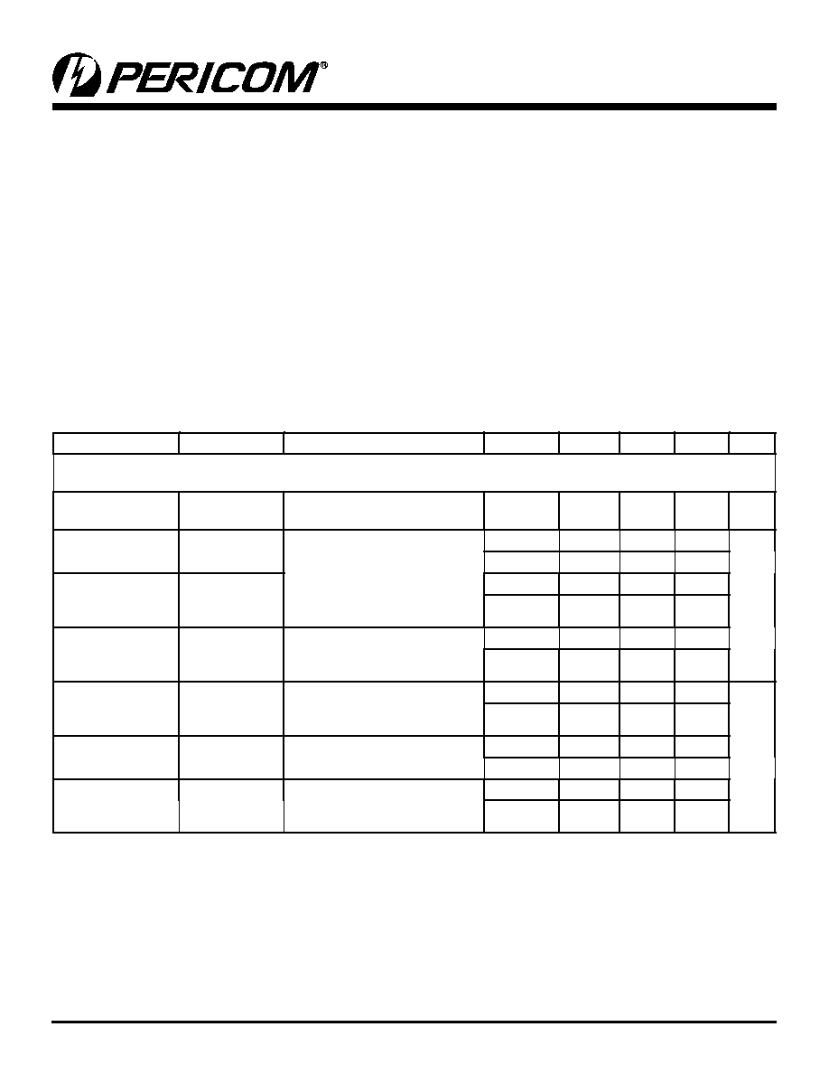
Electrical Specifications - Single +5V Supply
(V+ = +5V ± 10%, GND = 0V, V
INH
= 2.4V, V
INL
= 0.8V)
Parameter
Symbol
Conditions
Temp.(∞C) Min.
(1)
Typ.
(2)
Max.
(1)
Units
Analog Switch
Analog Signal
Range
(3)
V
ANALOG
Full
0
V+
V
On-Resistance
R
ON
V+ = 4.5V,
I
COM
= -30mA,
V
NO
or V
NC
= +2.5V
25
7.2
10
Full
12
On-Resistance
Match Between
Channels
(4)
R
ON
25
0.2
2
Full
4
On-Resistance Flat-
ness
(5)
R
FLAT(ON
)
V+ = 5V,
I
COM
= -30mA,
V
NO
or V
NC
= 1V, 2.5V, 4V
25
2.72
3.5
Full
4
NO or NC Off Leak-
age Current
(6)
I
NO(OFF)
or
I
NC(OFF)
V+ = 5.5V,
V
COM
= 0V,
V
NO
or V
NC
= 4.5V
25
0.18
nA
Full
-80
80
COM Off Leakage
Current
(6)
I
COM(OFF)
V+ = 5.5V, V
COM
= + 4.5V,
V
NO
or V
NC
= ± 0V
25
0.20
Full
-80
80
COM On Leakage
Current
(6)
I
COM(ON)
V+ = 5.5V,
V
COM
= +4.5V
V
NO
or V
NC
= +4.5V
25
0.20
Full
-80
80
3
PS8203G 10/19/04
PI5A121/PI5A122/PI5A124
Wide Bandwidth Analog Switch
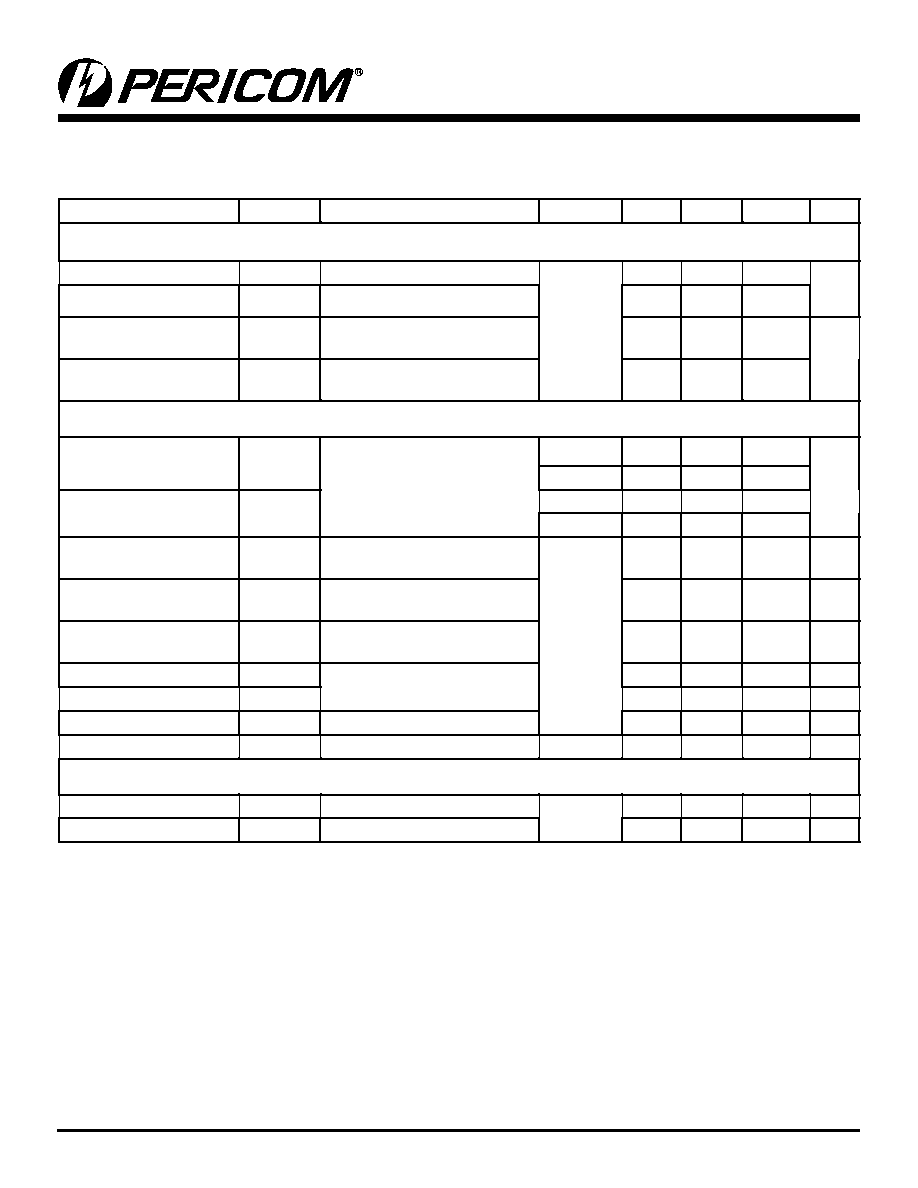
Electrical Specifications - Single +5V Supply
(continued)
(V+ = + 5V ± 10%, GND = 0V, V
INH
= 2.4V, V
INL
= 0.8V)
Parameter
Symbol
Conditions
Temp(∫C) Min.
(1)
Typ.
(2)
Max.
(1)
Units
Logic Input
Input High Voltage
V
IH
Guaranteed logic High Level
Full
2
V
Input Low Voltage
V
IL
Guaranteed logic Low Level
0.8
Input Current with Voltage
High
I
INH
V
IN
= 2.4V, all others = 0.8V
-1
0.005
1
µA
Input Current with Voltage
Low
I
INL
V
IN
= 0.8V, all others = 2.4V
-1
0.005
1
Dynamic
Turn-On Time
t
ON
V
CC
= 5V, Figure 1
25
7
15
ns
Full
20
Turn-Off Time
t
OFF
25
1
7
Full
10
Charge Injection
(3)
Q
C
L
= 1nF, V
GEN
= 0V,
R
GEN
= 0, Figure 2
25
1.6
10
pC
Off Isolation
O
IRR
R
L
= 50, C
L
= 5pF,
f = 10MHz, Figure 3
-43
dB
Crosstalk
(8)
X
TALK
R
L
= 50, C
L
= 5pF,
f = 10MHz, Figure 4
-43
NC or NO Capacitance
C
(OFF)
f = 1kHz, Figure 5
5.5
pF
COM Off Capacitance
C
COM(OFF)
5.5
COM On Capacitance
C
COM(ON)
f = 1kHz, Figure 6
13
-3dB Bandwidth
BW
R
L
= 50, Figure 7
Full
326
MHz
Supply
Power-Supply Range
V+
Full
2
6
V
Positve Supply Current
I+
V
CC
= 5.5V, V
IN
= 0V or V+
1
µA
Notes:
1. The algebraic convention, where most negative value is a minimum and most positive is a maximum, is used in this data sheet.
2. Typical values are for DESIGN AID ONLY, not guaranteed or subject to production testing.
3. Guaranteed by design
4. R
ON
=
R
ON
max - R
ON
min
5. Flatness is defined as the difference between the maximum and minimum value of On-Resistance measured.
6. Leakage parameters are 100% tested at maximum rated hot temperature and guaranteed by correlation at +25∫C.
7. Off Isolation = 20log
10
[ V
COM
/ (V
NO
or V
NC
)
]. See Figure 3.
8. Between any two switches. See Figure 4.
4
PS8203G 10/19/04
PI5A121/PI5A122/PI5A124
Wide Bandwidth Analog Switch
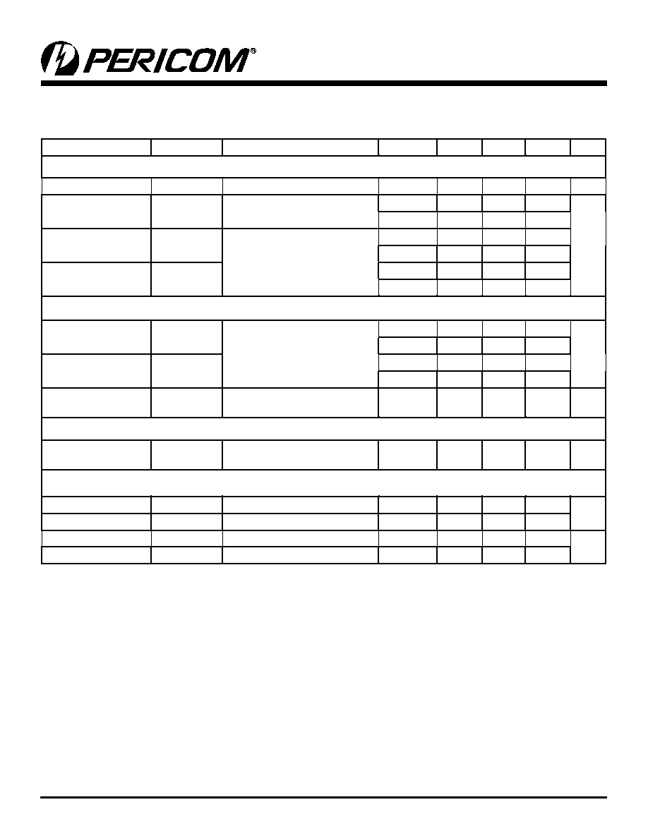
Electrical Specifications - Single +3.3V Supply
(V+ = +3.3V ± 10%, GND = 0V, V
INH
= 2.4V, V
INL
= 0.8V)
Parameter
Symbol
Conditions
Temp.(∫C) Min.(1) Typ.(2) Max.(1) Units
Analog Switch
Analog Signal Range
(3)
V
ANALOG
0
V+
V
On-Resistance
R
ON
V+ = 3V, I
COM
= -30mA,V
NO
or
V
NC
= 1.5V
25
12
18
Full
22
On-Resistance Match
Between Channels
(4)
R
ON
V+ = 3.3V, I
COM
= -30mA,
V
NO
or V
NC
= 0.8V, 2.5V
25
1
1
Full
2
On-Resistance Flat-
ness
(3,5)
R
FLAT(ON)
25
0.5
4
Full
5
Dynamic
Turn-On Time
t
ON
V+ = 3.3V,
V
NO
or V
NC
= 1.5V,
Figure 1
25
15
25
ns
Full
40
Turn-Off Time
t
OFF
25
1.5
12
Full
20
Charge Injection
(3)
Q
C
L
= 1nF, V
GEN
= 0V,
R
GEN
= 0V, Figure 2
25
1.3
10
pC
Supply
Positve Supply Current
I+
V+ = 3.6V, V
IN
= 0V or V+ All
Channels on or off
Full
1
µA
Logic Input
Input High Voltage
V
IH
Guaranteed logic high level
Full
2
V
Input Low Voltage
V
IL
Guaranteed logic low level
Full
0.8
Input High Current
I
INH
V
IN
= 2.4V, all others = 0.8V
Full
-1
1
µA
Input Low Current
I
INL
V
IN
= 0.8V, all others = 2.4V
Full
-1
1
5
PS8203G 10/19/04
PI5A121/PI5A122/PI5A124
Wide Bandwidth Analog Switch
Test Circuits/Timing Diagrams
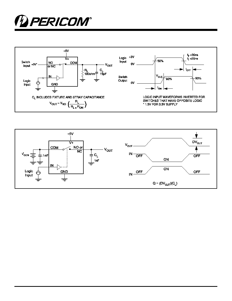
Figure 1. Switching Time
Figure 2. Charge Injection
6
PS8203G 10/19/04
PI5A121/PI5A122/PI5A124
Wide Bandwidth Analog Switch
Test Circuits/Timing Diagrams
(continued)
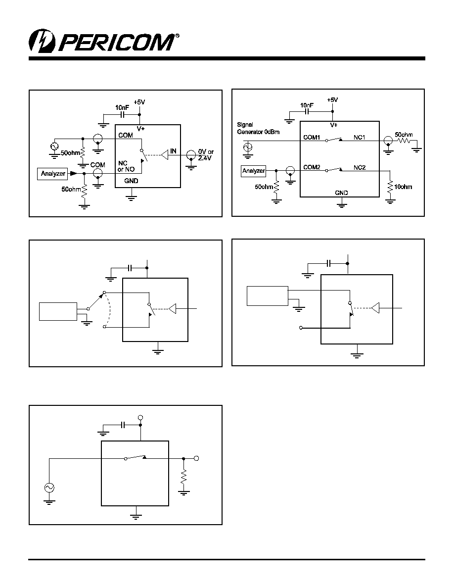
Figure 3. Off Isolation
Figure 5. Channel-Off Capacitance
Figure 4. Crosstalk (124 only)
Figure 6. Channel-On Capacitance
Figure 7. Bandwidth
V+
+5V
NC
Capacitance
Meter
GND
COM
10nF
IN
2.4V
f = 1kHz
V+
+5V
NC
Capacitance
Meter
GND
COM
10nF
IN
0V
f = 1MHz
V+
GND
NC or
NO
10nF
COM
+5V
Vo
Rg = 50ohm
R
L
50ohm
7
PS8203G 10/19/04
PI5A121/PI5A122/PI5A124
Wide Bandwidth Analog Switch
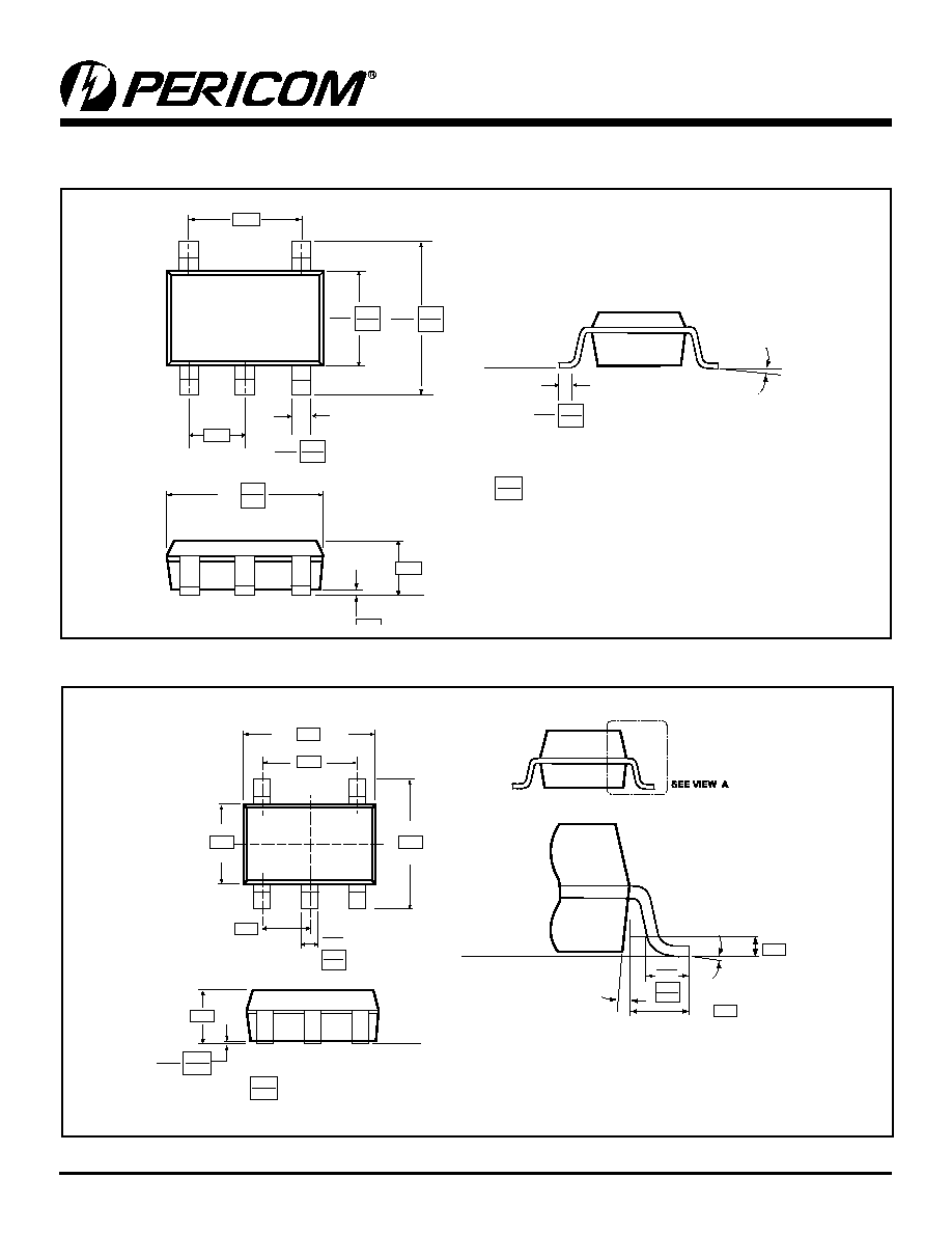
Packaging Mechanical: 5-pin SOT-23 (T)
.102
.118
BSC
0.60
1
2
3
.000
.005
0.00
0.15
.014
.019
0.35
0.50
5
4
1.50
1.75
.059
.068
0.10
.023
.004
1.45MAX.
SEATING
PLANE
.057
0∫ - 10∫
1.90
.075
.037
BSC
2.60
3.00
0.95
.110
.118
2.80
3.00
X.XX
X.XX
Datum "A"
DENOTES DIMENSIONS
IN MILIMETERS
Packaging Mechanical: 5-pin SC70 (C)
GUAGE PLANE
SEATING PLANE
SEATING PLANE
DENOTES DIMENSIONS
IN MILLIMETERS
BSC
VIEW A
BSC
REV
0
∞
-8
∞
4
∞
-10
∞
0.15
.321
0.42
.017
.010
.018
0.26
0.46
.006
3
4
5
2
1
.011
.026 0.65
BSC
.083
2.10
BSC
.049
1.25
BSC
.051
1.30
BSC
.079 2.00
0.15
0.30
MAX
.004 0.10
0
0
XXX
XXX
1.10
8
PS8203G 10/19/04
PI5A121/PI5A122/PI5A124
Wide Bandwidth Analog Switch
Ordering Information
Ordeing Code
Packaging Code
Package Type
Top Marking
PI5A121TX
T
5-pin, 65-mil wide SOT-23
ZV
PI5A121TEX
T
Pb-free & Green, 5-pin, 65-mil wide SOT-23
ZV
PI5A121CX
C
5-pin, 50-mil wide SOT-23
ZV
PI5A121CEX
C
Pb-free & Green, 5-pin, 50-mil wide SOT-23
ZV
PI5A122TX
T
5-pin, 65-mil wide SOT-23
ZU
PI5A122TEX
T
Pb-free & Green, 5-pin, 65-mil wide SOT-23
ZU
PI5A122CX
C
5-pin, 50-mil wide SOT-23
ZU
PI5A122CEX
C
Pb-free & Green, 5-pin, 50-mil wide SOT-23
ZU
PI5A124TX
T
6-pin, 65-mil wide SOT-23
ZT
PI5A124TEX
T
Pb-free & Green, 6-pin, 65-mil wide SOT-23
ZT
Notes:
1. Thermal characteristics can be found on the company web site at www.pericom.com/packaging/
2. X = Tape/Reel
Pericom Semiconductor Corporation ∑ 1-800-435-2336 ∑ www.pericom.com
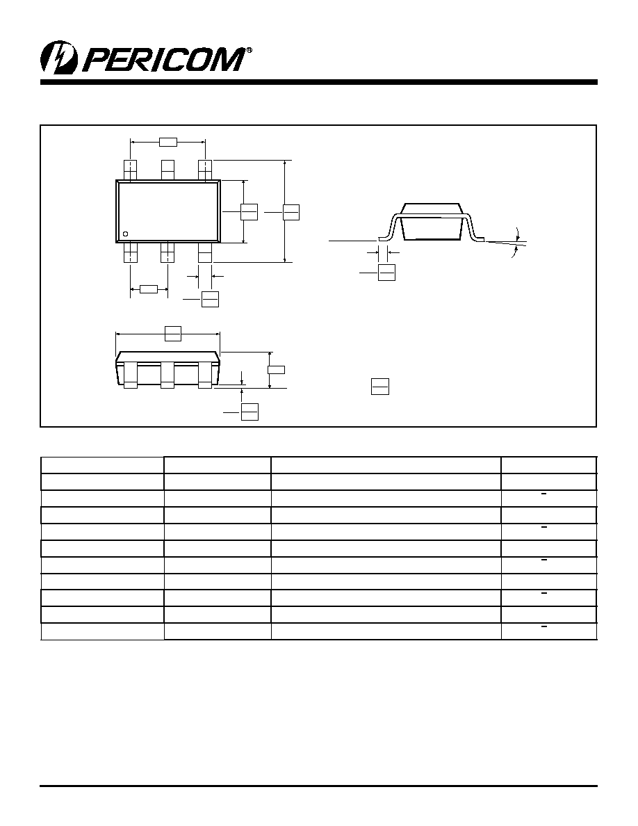
Packaging Mechanical: 6-pin SOT-23 (T)
0.102
0.118
BSC
0.60
0.000
0.005
0.00
0.15
0.014
0.019
0.35
0.50
1.50
1.75
0.059
0.068
0.10
0.023
0.004
1.45MAX.
SEATING
PLANE
0.057
0∫ - 10∫
1.90
0.075
0.037
BSC
2.60
3.00
0.95
0.110
0.118
2.80
3.00
X.XX
X.XX
Datum "A"
DENOTES DIMENSIONS
IN MILLIMETERS
2
5
3
6
4