 | –≠–ª–µ–∫—Ç—Ä–æ–Ω–Ω—ã–π –∫–æ–º–ø–æ–Ω–µ–Ω—Ç: PI5A3158 | –°–∫–∞—á–∞—Ç—å:  PDF PDF  ZIP ZIP |
1
PS8637B 07/26/04
Features
∑ CMOS Technology for Bus and Analog Applications
∑ Low On-Resistance: 8 at 3.0V
∑ Wide V
CC
Range: 1.65V to 5.5V
∑ Rail-to-Rail Signal Range
∑ Control Input Overvoltage Tolerance: 5.5V min.
∑ Fast Transition Speed: 5.2ns max. at 5V
∑ High Off Isolation: 57dB at 10MHz
∑ 54dB (10MHz) Crosstalk Rejection Reduces Signal Distortion
∑ Break-Before-Make Switching
∑ High Bandwidth: 250 MHz
∑ Extended Industrial Temperature Range: ≠40
∞
C to 85
∞
C
∑ Packaging (Pb-free & Green available):
-12-contact TDFN (ZA)
Applications
∑ Cell Phones
∑ PDAs
∑ Portable Instrumentation
∑ Battery Powered Communications
∑ Computer Peripherals
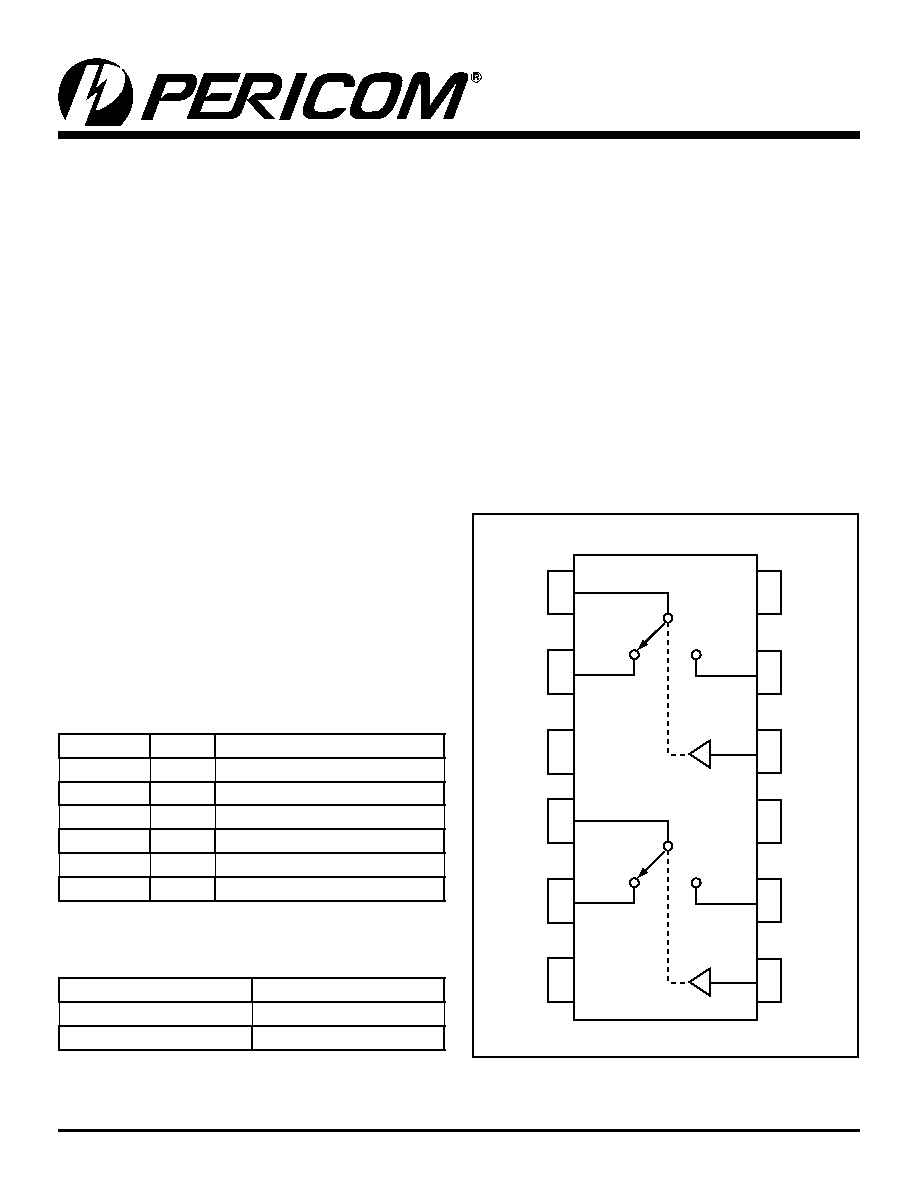
PI5A3158
SOT
INY
TM
Low Voltage Dual SPDT Analog Switch
2:1 Mux/DeMux Bus Switch
Description
The PI5A3158 is a dual high-bandwidth, fast single-pole double-
throw (SPDT) CMOS switch. It can be used as an analog switch or
as a low-delay bus switch. Specified over a wide operating power
supply voltage range, 1.65V to 5.5V, the PI5A3158 has a maximum
On-Resistance of 12 at 1.65V, 9 at 2.3V & 6 at 4.5V.
Break-before-make switching prevents both switches being
enabled simultaneously. This eliminates signal disruption during
switching.
The control input, S, tolerates input drive signals up to 5.5V,
independent of supply voltage.
Logic Function Table
Pin Description
Connection Diagram
Notes:
1. x = 0 or 1
1B0
GND
1
2
3
12
10
0B0
GND
0B1
1B1
S0
11
VCC
VCC
A0
S1
A1 4
5
6
9
7
8
Logic Input(s)
Function
0
0
B
X
Connection to A
X
1
1
B
X
Connected to A
X
Pin Number Name
Description
8, 11
1
B
X
Data port (Normally Open)
3, 6
GND
Ground
2, 5
0
B
X
Data port (Normally Closed)
1, 4
A
X
Common Output/data port
9, 12
V
CC
Positive Power Supple
7, 10
S
X
Logic Controll
2
PS8637B 07/26/04
PI5A3158
SOT
INY
TM
Low Voltage Dual SPDT Analog Switch
2:1 Mux/DeMux Bus Switch
Recommended Operating Conditions
(3)
Supply Voltage Operating (V
CC
) . . . . . . . . . . . . 1.65V to 5.5V
Control Input Voltage (V
IN
) . . . . . . . . . . . . . . . . . . . 0V to V
CC
Switch Input Voltage (V
IN
). . . . . . . . . . . . . . . . . . . . 0V to V
CC
Output Voltage (V
OUT
) . . . . . . . . . . . . . . . . . . . . . . . 0V to V
CC
Operating Temperature (T
A
) . . . . . . . . . . . . . . . ≠40∞C to +85∞C
Input Rise and Fall Time (t
r
,t
f
)
Control Input V
CC
= 2.3V - 3.6V. . . . . . . . . 0ns/V to 10ns/V
Control Input V
CC
= 4.5V - 5.5V. . . . . . . . . . 0ns/V to 5ns/V
Thermal Resistance (
JA
) . . . . . . . . . . . . . . . . . . . . . . 350∞C/W
Absolute Maximum Ratings
(1)
Supply Voltage V
CC
............................................ ≠0.5V to +7V
DC Switch Voltage (V
S
)
(2)
........................≠0.5V to V
CC
+0.5V
DC Input Voltage (V
IN
)
(2)
................................ ≠0.5V to +7.0V
DC Output Current (V
OUT
) ........................................... 128mA
DC V
CC
or Ground Current (I
CC
/I
GND
)
....................... ±100mA
Storage Temperature Range (T
STG
) .............. ≠65∞C to +150∞C
Junction Temperature under Bias (T
J
) .............................150∞C
Junction Lead Temperature (T
L
)
(Soldering, 10 seconds) ................................................260∞C
Power Dissipation (P
D
) @ +85∞C .................................. 180mW
Notes:
1. Absolute Maximum Ratings" may cause permanent damage to the device. This is a stress only rating and operation of the device at these or any
other conditions beyond those indicated in the operational sections of this specification is not implied.
2. The input and output negative voltage ratings may be exceeded if the inut and output diode current ratings are observed.
3. . . . . . . Control input must be held HIGH or LOW; it must not float.
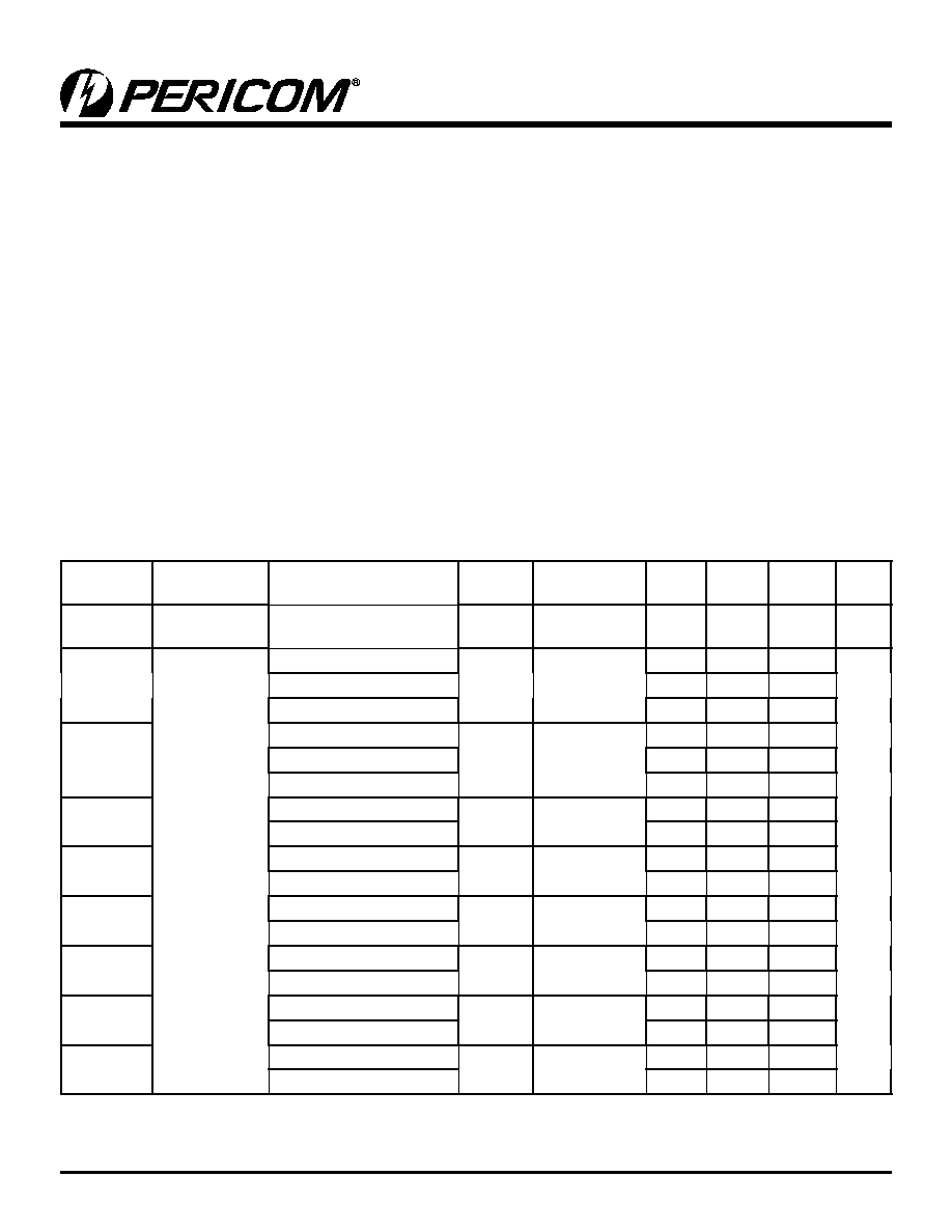
DC Electrical Characteristics
(Over the Operating temperature range, T
A
= ≠40∞C to 85∞C)
Parameters
Description
Test Conditions
Supply
Voltage
Temp
Min.
Typ.
Max.
Units
V
IAR
Analog Input
Signal Range
V
CC
T
A
= 25∫C &
-40∫C to 85∫C
0
V
CC
V
R
ON
On-
Resistance
(4)
I
O
= 30mA, V
IN
= 0V
4.5V
T
A
= 25∫C
4
6
I
O
= -30mA, V
IN
= 2.4V
5
8
I
O
= -30mA, V
IN
= 4.5V
8
13
R
ON
I
O
= 30mA, V
IN
= 0V
4.5V
T
A
= -40∫C to
85∫C
6
I
O
= -30mA, V
IN
= 2.4V
8
I
O
= -30mA, V
IN
= 4.5V
13
R
ON
I
O
= 24mA, V
IN
= 0V
3.0V
T
A
= 25∫C
5
8
I
O
= -24mA, V
IN
= 3.0V
12
19
R
ON
I
O
= 24mA, V
IN
= 0V
3.0V
T
A
= -40∫C to
85∫C
8
I
O
= -24mA, V
IN
= 3.0V
19
R
ON
I
O
= 24mA, V
IN
= 0V
2.3V
T
A
= 25∫C
6
9
I
O
= -24mA, V
IN
= 2.3V
16
24
R
ON
I
O
= 24mA, V
IN
= 0V
2.3V
T
A
= -40∫C to
85∫C
9
I
O
= -24mA, V
IN
= 2.4V
24
R
ON
I
O
= 24mA, V
IN
= 0V
1.65V
T
A
= 25∫C
8
12
I
O
= -24mA, V
IN
= 1.65V
27
39
R
ON
I
O
= 24mA, V
IN
= 0V
1.65V
T
A
= -40∫C to
85∫C
12
I
O
= -24mA, V
IN
= 1.65V
39
3
PS8637B 07/26/04
PI5A3158
SOT
INY
TM
Low Voltage Dual SPDT Analog Switch
2:1 Mux/DeMux Bus Switch
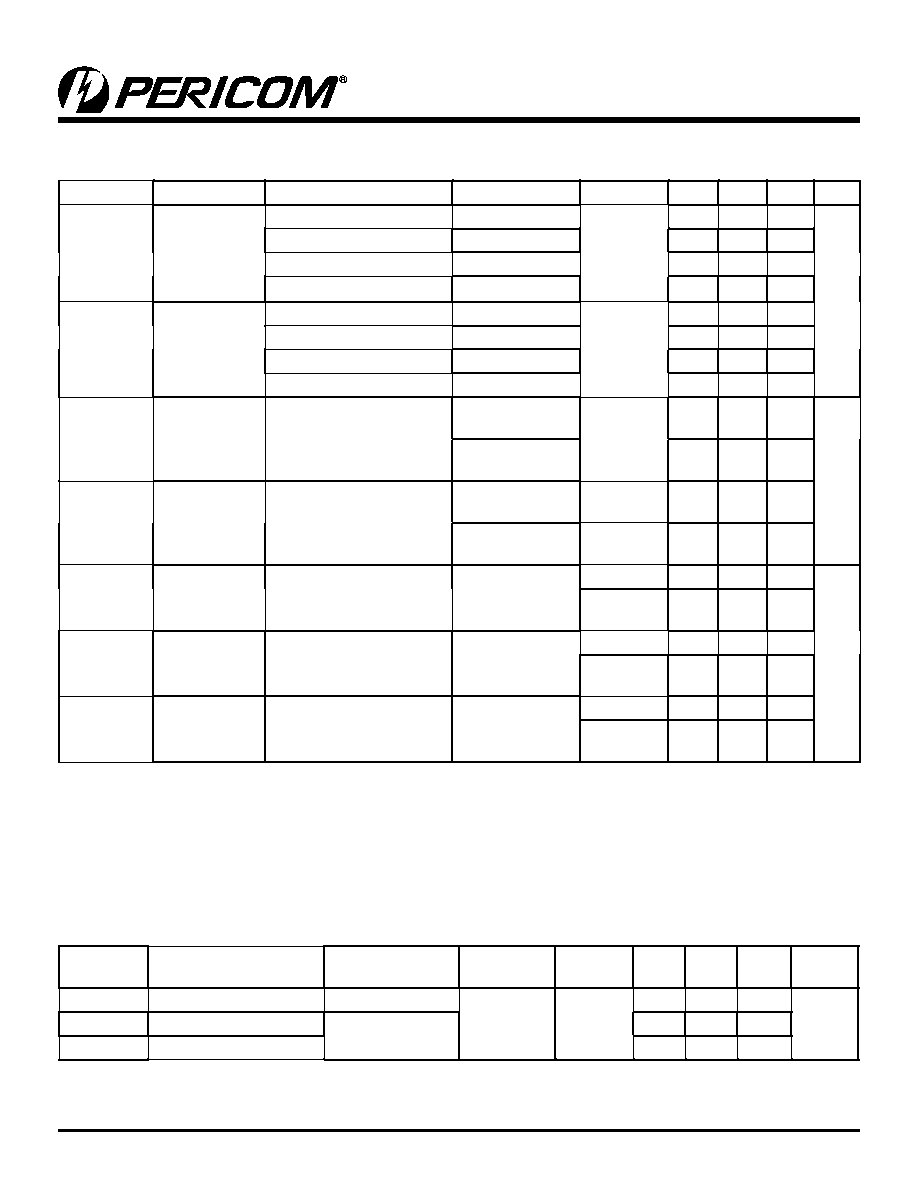
DC Electrical Characteristics
(Over the Operating temperature range, T
A
= ≠40∞C to 85∞C) (continued)
Parameters
Description
Test Conditions
Supply Voltage
Temp
Min. Typ. Max. Units
R
ON
On-Resistance
Match Between
Channels
(4, 5, 6)
I
A
= -30mA, V
BN
= 3.15V
4.5V
T
A
= 25∫C
0.15
I
A
= -24mA, V
BN
= 2.1V
3.0V
0.2
I
A
= -8mA, V
BN
= 1.6V
2.3V
0.3
I
A
= -4mA, V
BN
= 1.15V
1.65V
0.3
R
ONF
On-Resistance
Flatness
(4, 5, 7)
I
A
= -30mA, 0 V
BN
V
CC
5.0V
T
A
= 25∫C
6
I
A
= -24mA, 0 V
BN
V
CC
3.3V
12
I
A
= -8mA, 0 V
BN
V
CC
2.5V
22
I
A
= -4mA, 0 V
BN
V
CC
1.8V
90
V
IH
Input High Volt-
age
Logic High Level
V
CC
= 1.65V to
1.95V
T
A
= -40∫C
to 85∫C
0.75
V
CC
V
V
CC
= 2.3V to
5.5V
0.7
V
CC
V
IL
Input Low Volt-
age
Logic LowLevel
V
CC
= 1.65V to
1.95V
V
CC
= 2.3V to
5.5V
Input Leakage
Curent
0 V
IN
5.5V
V
CC
0V 5.5V
T
A
= 25∫C
±0.1
µA
T
A
= -40∫C
to 85∫C
±1.0
I
OFF
OFF State
Leakage Cur-
rent
0 V
IN
5.5V
V
CC
1.65V
5.5V
T
A
= 25∫C
±0.1
T
A
= -40∫C
to 85∫C
±10
I
CC
Quiescent Sup-
ply Current
All Channels ON or OFF,
V
IN
= V
CC
or GND, I
OUT
= 0
V
CC
= 5.5V
T
A
= 25∫C
2
T
A
= -40∫C
to 85∫C
20
Notes:
4. Measured by voltage drop between A and B pins at the indicated current through the device. On-Resistance is determined by the lower of the
voltages on two ports (A or B).
5. Parameter is characterized but not tested in production.
6. R
ON
= R
ON
max ≠ R
ON
min. measured at identical V
CC
, temperature and voltage levels.
7. Flatness is defined as difference between maximum and minimum value of On-Resistance over the specified range of conditions.
8. Guaranteed by design.
Capacitance
(12)
Parameters
Description
Test Conditions
Supply
Voltage
Temp
Min.
Typ.
Max.
Units
C
IN
Controll Input
V
CC
= 5.0V
T
A
= 25∫C
2.3
pF
C
IO-B
For B Port, Switch OFF
f = 1 MHz
(12)
6.5
C
IOA-ON
For A Port, Switch ON
18.5
4
PS8637B 07/26/04
PI5A3158
SOT
INY
TM
Low Voltage Dual SPDT Analog Switch
2:1 Mux/DeMux Bus Switch
Switch and AC Characteristics
Parameters
Description
Test Conditions
Supply
Voltage
Temp
Min.
Typ.
Max. Units
t
PLH
t
PHL
Propagation
Delay: A to Bn
See test circut
diagram 1 and 2
V
I
Open
(10)
V
CC
= 2.3V to 2.7V
T
A
= 25∫C &
-40∫C to 85∫C
1.2
V
CC
= 3.0V to 3.6V
0.8
V
CC
= 4.5V to 5.5V
0.3
t
PZL
t
PZH
Output Enable
Turn ON Time:
A to Bn
See test circut
diagram 1 and 2
V
I
= 2 V
CC
for
t
PZL
, V
I
= 0V for
t
PZH
V
CC
= 1.65V to 1.95V
T
A
= 25∫C
7
23
V
CC
= 2.3V to 2.7V
3.5
13
V
CC
= 3.0V to 3.6V
2.5
6.9
V
CC
= 4.5V to 5.5V
1.7
5.2
t
PZL
t
PZH
Output Enable
Turn ON Time:
A to Bn
See test circut
diagram 1 and 2
V
I
= 2 V
CC
for
t
PZL
, V
I
= 0V for
t
PZH
V
CC
= 2.5V
T
A
= 25∫C &
-40∫C to 85∫C
24
V
CC
= 3.3V
14
V
CC
= 3.0V to 3.6V
7.6
V
CC
= 4.5V to 5.5V
5.7
t
PLZ
t
PHZ
Output Disable-
Turn OFF Time:
A to Bn
See test circut
diagram 1 and 2
V
I
= 2 V
CC
for
t
PZL
, V
I
= 0V for
t
PZH
V
CC
= 1.65V to 1.95V
T
A
= 25∫C
3
12.5
V
CC
= 2.3V to 2.7V
2
7
V
CC
= 3.0V to 3.6V
1.5
5
V
CC
= 4.5V to 5.5V
0.8
3.5
t
PLZ
t
PHZ
Output Disable-
Turn OFF Time:
A to Bn
See test circut
diagram 1 and 2
V
I
= 2 V
CC
for
t
PZL
, V
I
= 0V for
t
PZH
V
CC
= 2.5V
T
A
= 25∫C &
-40∫C to 85∫C
13
V
CC
= 3.3V
7.5
V
CC
= 3.0V to 3.6V
5.3
V
CC
= 4.5V to 5.5V
3.8
t
BM
Break Before
Make Time
See Test Circut
diagram 9.
(9)
V
CC
= 2.5V
T
A
= 25∫C &
-40∫C to 85∫C
0.5
V
CC
= 3.3V
0.5
V
CC
= 3.0V to 3.6V
0.5
V
CC
= 4.5V to 5.5V
0.5
Q
Charge Injection
C
L
= 0.1nF,
V
GEN
= 0V,
R
GEN
= 0, See
test circut 4
V
CC
= 5.0V
T
A
= 25∫C
7
pC
V
CC
= 3.3V
3
O
IRR
Off Isolation
R
L
= 50,
V
GEN
= 0V,
R
GEN
= 0, See
test circut 5
(11)
V
CC
= 1.65V to 5.5V
T
A
= 25∫C
-57
dB
X
TALK
Crosstalk Isola-
tion
See test circut 6
V
CC
= 1.65V to 5.5V
T
A
= 25∫C
-54
f
3dB
-3dB Bandwidth See test circut 9
V
CC
= 1.65V to 5.5V
T
A
= 25∫C
250
MHz
Notes:
9. Guaranteed by design.
10. Guaranteed by design but not production tested. The device contributes no other propagation delay other than the RC delay of the switch On-
Resistance and the 50pF load capacitance, whne driven by an ideal voltage source with zero output impedance.
11. Off Isolation = 20 Log
10
[ V
A
/ V
Bn
] and is measured in dB.
12. T
A
= 25∞C, f = 1MHz. Capacitance is characterized but not tested in production.
5
PS8637B 07/26/04
PI5A3158
SOT
INY
TM
Low Voltage Dual SPDT Analog Switch
2:1 Mux/DeMux Bus Switch
100
CL
10pF
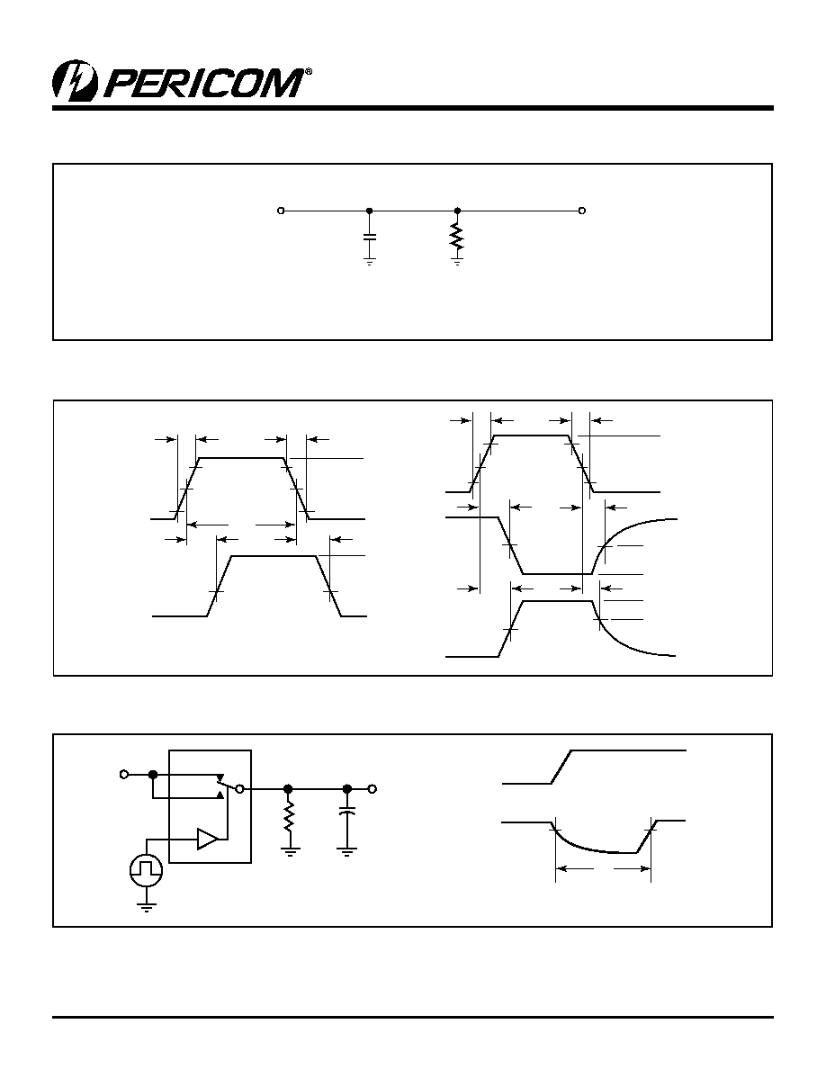
Notes: Input driven by 50W source terminated in 50.
CL includes load and stray capacitance.
Input PRR = 1.0 MHz; tw = 500ns.
From
Output
Under
Test
Figure 1. AC Test Circuit
Figure 2. AC Waveforms
tr = 2.5ns
10%
10%
10%
10%
50%
V
CC
V
CC
V
OL
+0.3V
V
OH
≠0.3V
V
OL
V
OH
V
TRI
V
TRI
V
OH
t
W
t
PLH
t
PHL
V
OL
GND
GND
90%
50%
50%
50%
90%
50%
90%
90%
50%
50%
50%
tr = 2.5ns
tr = 2.5ns
tr = 2.5ns
t
PZL
t
PZH
t
PHZ
t
PLZ
SWITCH
INPUT
OUTPUT
CONTROL
INPUT
OUTPUT
OUTPUT
Figure 3. Break Before Make Interval Timing
Test Circuits and Timing Diagrams
C
L
R
L
t
D
V
OUT
0.9 x V
OUT
Logic
Input
A
A
B
0
B
1
V
IN
Logic
Input
V
OUT
6
PS8637B 07/26/04
PI5A3158
SOT
INY
TM
Low Voltage Dual SPDT Analog Switch
2:1 Mux/DeMux Bus Switch
Figure 4. Charge Injection Test
C
L
R
L
1M
100pF
A
S
B
N
V
GE
R
GEN
Logic
Input
Logic
Input
Q = (
V
OUT
)(C
L
)
V
OUT
OFF
ON
OFF
V
OUT
Figure 5. Off Isolation
Analyzer
A
S
10nF
GND
B
N
V
CC
V
CC
Logic Input
0V or B
IH
50
50
Figure 6. Crosstalk
Analyzer
Signal
Generator
0dBm
S
A
10nF
GND
B
0
B
1
V
CC
V
CC
50
50
Figure 7. Channel Off Capacitance
Figure 8. Channel On Capacitance
Capacitance
Meter
A
S
10nF
GND
f = 1 MHz
B
N
V
CC
V
CC
Logic Input
0V or B
IH
Capacitance
Meter
A
S
10nF
GND
B
N
V
CC
V
CC
f = 1 MHz
Logic Input
0V or B
IH
7
PS8637B 07/26/04
PI5A3158
SOT
INY
TM
Low Voltage Dual SPDT Analog Switch
2:1 Mux/DeMux Bus Switch
Pericom Semiconductor Corporation ∑ 1-800-435-2336 ∑ www.pericom.com
Figure 9. Bandwidth
Signal
Generator
0dBm
A
10nF
GND
B
N
Logic Input
0V or V
CC
S
V
CC
V
CC
50
0.0 - 0.05
3.00 ± 0.10
1.00 ± 0.10
0.20 ± 0.05 (12x)
2.50 Ref. (2x)
0.50 Typ.
0.15
0.30 ± 0.10 (12X)
Pin 1
0.80 MAX
0.80 MAX
Packaging Mechanical : 12-contact TDFN (ZA)
Ordering Information
Ordering Code
Packaging Code
Package Type
PI5A3158ZA
(1)
ZA
12-contact TDFN
PI5A3158ZAE
ZA
Pb-free & Green, 12-contact TDFN
Notes:
1. This product has always shipped as only a lead free product, but since it was introduced prior to Pericom's strategy of adding an E to all Green/
Lead free parts many customers order it without the E suffix. Please migrate new designs and qualification to include the E suffix. Pericom at
this point in time will continue to offer devices marked both ways, but may at a later date eliminate the non-E part number.
2. Thermal characteristics can be found on the company web site at www.pericom.com/packaging/